-
TPS7B4250-Q1 50-mA 40-V Voltage-Tracking LDO With 5-mV Tracking Tolerance
- 1 Features
- 2 Applications
- 3 Description
- 4 Revision History
- 5 Pin Configuration and Functions
- 6 Specifications
- 7 Detailed Description
- 8 Application and Implementation
- 9 Power Supply Recommendations
- 10Layout
- 11Device and Documentation Support
- 12Mechanical, Packaging, and Orderable Information
- IMPORTANT NOTICE
TPS7B4250-Q1 50-mA 40-V Voltage-Tracking LDO With 5-mV Tracking Tolerance
1 Features
- Qualified for Automotive Applications
- AEC-Q100 Qualified With the Following Results
- –20-V to 45-V Wide, Maximum Input Voltage Range
- Output Current, 50 mA
- Very-Low Output-Tracking Tolerance,
5 mV (max) - 150-mV Low Dropout Voltage When
IOUT = 10 mA - Combined Reference and Enable Input
- 40-µA Low Quiescent Current at Light Load
- Extreme, Wide ESR Range.
- Stable with 1-µF to 50-µF Ceramic Output Capacitor, ESR 1 mΩ to 20 Ω
- Reverse Polarity Protection
- Overtemperature Protection
- Output Short-Circuit Proof to Ground and Supply
- SOT-23 Package
2 Applications
- Off-board Sensor Supply
- High-Precision Voltage Tracking
3 Description
The TPS7B4250-Q1 device is a monolithic, integrated low-dropout voltage tracker. The device is available in a SOT-23 package. The TPS7B4250-Q1 device is designed to supply off-board sensors in an automotive environment. The IC has integrated protection for overload, over temperature, reverse polarity, and output short-circuit to the battery and ground.
A reference voltage applied at the adjust-input pin, ADJ, regulates supply voltages up to VIN = 45 V with high accuracy and loads up to 50 mA.
By setting the adjust/enable input pin, ADJ/EN, to low, the TPS7B4250-Q1 device switches to standby mode which reduces the quiescent current to the minimum value.
Device Information(1)
| PART NUMBER | PACKAGE | BODY SIZE (NOM) |
|---|---|---|
| TPS7B4250-Q1 | SOT-23 (5) | 2.90 mm × 1.60 mm |
- For all available packages, see the orderable addendum at the end of the data sheet.
4 Revision History
Changes from B Revision (July 2015) to C Revision
- Changed the title of the data sheet Go
- Added the Device Support and Receiving Notification of Documentation Updates sectionsGo
Changes from A Revision (November 2013) to B Revision
- Changed HBM ESD Classification level from 2 to 3A Go
- Changed CDM ESD Classification level from C4 to C6Go
- Added Pin Configuration and Functions section, ESD Ratings table, Feature Description section, Device Functional Modes, Application and Implementation section, Power Supply Recommendations section, Layout section, Device and Documentation Support section, and Mechanical, Packaging, and Orderable Information sectionGo
- Deleted the transient current and 107-pF capacitor for HBM table notes from the ESD Ratings table Go
- Changed input voltage symbol from VIN to VI for the ΔVO(ΔVI) and Vdropout parameters and the output voltage symbol from VOUT to VO for the IL parameter in the Electrical Characteristics tableGo
- Added IO and CO to the PSRR test condition in the Electrical Characteristics table Go
- Changed the max value for Vdropout where IO = 10 mA from 250 to 265 in the Electrical Characteristics tableGo
- Deleted the VADJ = 5 V condition for the Ground current vs Temperature graph and changed the legendGo
- Changed the y axis units from mV to mA in the Current-limit vs Temperature graph Go
- Added the VADJ condition statement to the Input Voltage vs Output Voltage graph and changed the y-axis from IO to VOGo
- Changed the title of Figure 8 from Input Voltage vs Output Voltage to Reference Voltage vs Output Voltage, and changed the y-axis from IO to VO. Also added the VI condition statement to the graphGo
- Changed the second y axis from IO to VI and removed the units in the Line TransientGo
- Deleted the units from the second y axis in the Load TransientGo
- Added the VADJ condition statement to the Power-supply Rejection Ratio vs Frequency graphGo
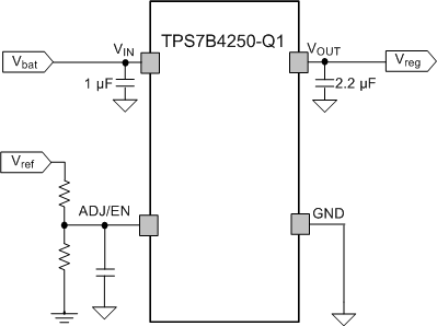
- Added resistor-divider values to the Tracking LDO With Enable Circuit figureGo
Changes from * Revision (October 2013) to A Revision
- Changed CDM ESD Classification level from C3B to C4 throughout documentGo
- Changed VOUT min value from –0.3 to –1 in the Absolute Maximum Ratings tableGo
- Added transient current flow to ESD rating in the Absolute Maximum Ratings tableGo
- Changed HBM absolute maximum rating from 2 kV to 4 kVGo
- Deleted relevant ESR value from Recommended Operating Conditions tableGo
- Added grater-than-or-equal-to (≥) value to VADJ/EN in condition statement of the Electrical Characteristics table Go
- Added VADJ = 1.5 V to both test conditions for VUVLO parameter in the Electrical Characteristics tableGo
- Changed max value for load regulation parameter from 3 to 4 in the Electrical Characteristics tableGo
- Changed max value for the current consumption test condition where IO = 0.5 mA from 80 to 90 in the Electrical Characteristics tableGo
- Added the Detailed Description sectionGo
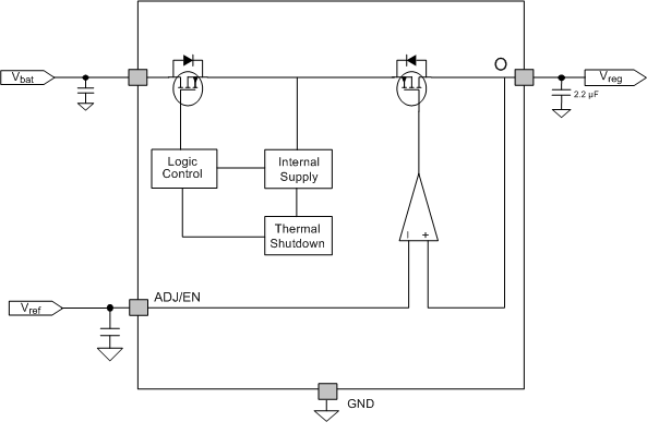
- Added the TPS7B4250 block diagramGo
5 Pin Configuration and Functions
Pin Functions
| PIN | TYPE | DESCRIPTION | |
|---|---|---|---|
| NAME | NO. | ||
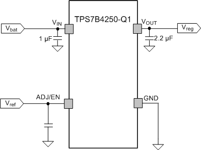
| ADJ/EN | 1 | I | This pin connects to the reference voltage. A low signal disables the IC and a high signal enables the device. Connected the voltage reference directly or with a voltage divider for lower output voltages. To compensate for line influences, TI recommends to place a capacitor close to the IC pins. |
| GND | 2 | G | Internally connected to pin 5 |
| GND | 5 | G | Internally connected to pin 2 |
| VIN | 3 | I | This pin is the device supply. To compensate for line influences, TI recommends to place a capacitor close to the IC pins. |
| VOUT | 4 | O | VOUT is an external capacitor that is required between VOUT and GND with respect to the capacitance and ESR requirements given in the Recommended Operating Conditions. |
6 Specifications
6.1 Absolute Maximum Ratings
over operating free-air temperature range (unless otherwise noted)(1)| MIN | MAX | UNIT | |||
|---|---|---|---|---|---|
| Input voltage, unregulated input, VIN(2)(3) | –20 | 45 | V | ||
| Output voltage, regulated output, VOUT | –1 | 22 | V | ||
| Adjust input and enable input voltage, ADJ/EN(2)(3) | –0.3 | 22 | V | ||
| ADJ Voltage minus input voltage (ADJ–VIN), VIN > 0 V | 7 | V | |||
| Operating junction temperature, TJ | –40 | 150 | °C | ||
| Storage temperature, Tstg | –65 | 150 | °C | ||
6.2 ESD Ratings
| VALUE | UNIT | |||
|---|---|---|---|---|
| V(ESD) | Electrostatic discharge | Human-body model (HBM), per AEC Q100-002(1) | ±4000 | V |
| Charged-device model (CDM), per AEC Q100-011 | ±1000 | |||
6.3 Recommended Operating Conditions
over operating free-air temperature range (unless otherwise noted)(2)| MIN | MAX | UNIT | ||
|---|---|---|---|---|
| VIN | Unregulated input | 4 | 40 | V |
| VOUT | regulated output | 1.5 | 18 | V |
| ADJ/EN | Adjust input and enable input voltage | 1.5 | 18 | V |
| ADJ–VIN | ADJ voltage minus input voltage | 5 | V | |
| COUT | Output capacitor requirements(1) | 1 | 50 | µF |
| ESRCOUT | Output ESR requirements | 0.001 | 20 | Ω |
| TJ | Operating junction temperature | –40 | 150 | °C |
6.4 Thermal Information
| THERMAL METRIC(2)(1) | TPS7B4250-Q1 | UNIT | |
|---|---|---|---|
| DBV (SOT-23) | |||
| 5 PINS | |||
| RθJA | Junction-to-ambient thermal resistance | 171.7 | °C/W |
| RθJC(top) | Junction-to-case (top) thermal resistance | 81.1 | °C/W |
| RθJB | Junction-to-board thermal resistance | 31.7 | °C/W |
| ψJT | Junction-to-top characterization parameter | 4.5 | °C/W |
| ψJB | Junction-to-board characterization parameter | 31.2 | °C/W |
| RθJC(bot) | Junction-to-case (bottom) thermal resistance | N/A | °C/W |
6.5 Electrical Characteristics
VI = 13.5 V, 18 V ≥ VADJ/EN ≥ 1.5 V, TJ = –40ºC to 150ºC unless otherwise stated| PARAMETER | TEST CONDITIONS | MIN | TYP | MAX | UNIT | |
|---|---|---|---|---|---|---|
| VUVLO | VIN undervoltage detection | Ramp up VI until the output turns on, VADJ = 1.5 V | 3.65 | V | ||
| Ramp down VI until the output turns off, VADJ = 1.5 V | 3 | |||||
| ΔVO | Output-voltage tracking accuracy | IO = 100 µA to 1 mA, VI = 4 V to 40 V, 1.5 V < VADJ < VI – 0.3 V | –4 | 4 | mV | |
| IO = 1 mA to 50 mA, VI = 4 V to 40 V, 1.5 V < VADJ < VI – 1.5 V | –5 | 5 | ||||
| ΔVO(ΔIL) | Load regulation steady-state | IO = 1 mA to 30 mA | 4 | mV | ||
| ΔVO(ΔVI) | Line regulation steady-state | IO = 10 mA, VI = 6 V to 40 V | 3 | mV | ||
| PSRR | Power-supply ripple rejection | Frequency = 100 Hz, Vrip = 0.5 VPP, IO = 5 mA, CO = 2.2 µF | 60 | dB | ||
| Vdropout | Dropout voltage, Vdropout = VI – VQ | IO = 10 mA, VI ≥ 4 V(1) | 150 | 265 | mV | |
| IO = 50 mA, VI ≥ 4 V(1) | 550 | 1000 | ||||
| IL | Output-current limitation | VO short to GND | 100 | 500 | mA | |
| IR | Reverse current at VIN | VI = 0 V, VO = 20 V, VADJ = 5 V | –5 | 0 | µA | |
| IRN1 | Reverse current at negative input voltage | VI = –20 V, VO = 0 V, VADJ = 5 V | –5 | 0 | µA | |
| IRN2 | VI = –20 V, VO = 20 V, VADJ = 5 V | –5 | 0 | |||
| TSD | Thermal shutdown temperature | TJ increasing because of power dissipation generated by the IC | 175 | °C | ||
| IQ | Current consumption | VADJ < 0.8 V, TA ≤ 85°C(2) | 7.5 | 15 | µA | |
| VADJ < 0.8 V, TA ≤ 125°C | 20 | |||||
| IO = 0.5 mA, VADJ = 5 V | 40 | 90 | ||||
| IO = 30 mA, VADJ = 5 V | 150 | 350 | ||||
| IADJ | Adjust-input and enable-input current | VADJ = 5 V | 1 | µA | ||
| VADJ,low | Adjust and enable low signal valid | VO = 0 V | 0.8 | V | ||
| VADJ,high | Adjust and enable high signal valid | |VO – VADJ| < 5 mV | 1.5 | 18 | V | |
6.6 Typical Characteristics

| VI = VADJ = 4 V | IO = 10 mA | |

| VI = 13.5 V | VADJ = 5 V | |

| VI = VADJ = 4 V | ||

| VI = 13.5 V | VADJ = 5 V | IO = 1 mA, 50 mA |

7 Detailed Description
7.1 Overview
The TPS7B4250-Q1 device is a monolithic integrated low-dropout voltage tracker with ultra-low tracking tolerance. Several types of protection circuits are also integrated in the device such as output current limitation, reverse polarity protection, and thermal shutdown in case of over temperature.
7.3 Feature Description
7.3.1 Regulated Output (VOUT)
VOUT is the regulated output based on the reference voltage. The output has current limitation. During initial power up, the regulator has an incorporated soft start to control the initial current through the pass element.
7.3.2 Undervoltage Shutdown
The device has an internally-fixed undervoltage shutdown threshold. Undervoltage shutdown activates when the input voltage on VIN drops below UVLO. This activation ensures the regulator is not latched into an unknown state during low input supply voltage. If the input voltage has a negative transient that drops below the UVLO threshold and recovers, the regulator shuts down and powers up similar to a standard power-up sequence when the input voltage is above the required levels.
7.3.3 Thermal Protection
Thermal protection disables the output when the junction temperature rises to approximately 175°C which allows the device to cool. When the junction temperature cools to approximately 150°C, the output circuitry enables. Based on power dissipation, thermal resistance, and ambient temperature, the thermal protection circuit may cycle on and off. This cycling limits the dissipation of the regulator and protects it from damage as a result of overheating.
The internal protection circuitry of the TPS7B4250-Q1 device has been designed to protect against overload conditions. The circuitry was not intended to replace proper heat-sinking. Continuously running the TPS7B4250-Q1 device into thermal shutdown degrades device reliability.
7.3.4 VOUT Short to Battery
The TPS7B4250-Q1 device survives a short to battery when the output is shorted to the battery as shown in Figure 13. No damage occurs to the device. A short to the battery can also occur when the device is powered by an isolated supply at a lower voltage as shown in Figure 14. In this case the TPS7B4250-Q1 supply input voltage is set at 7 V when a short to battery (14 V typical) occurs on VOUT which typically runs at 5 V. The continuous reverse current flows out through VIN is less than 5 µA.
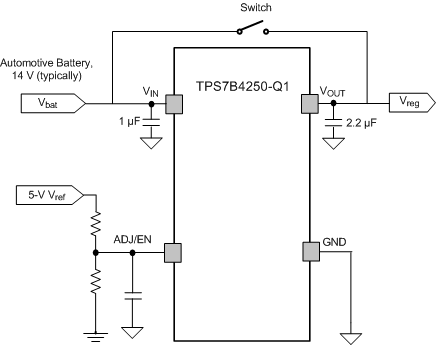 Figure 13. Output-Voltage Short to Battery
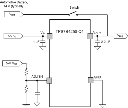 Figure 14. Output Voltage Higher than Input
7.3.5 Tracking Regulator with ENABLE Circuit
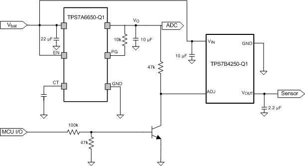
By pulling the reference voltage of the device below 0.8 V, the IC disables and enters a sleep state where the device draws 7.5 µA (typical) from the power supply. In a real application, the reference voltage is generally sourced from another LDO voltage rail. A case where the device must be disabled without a shutdown of the reference voltage can occur. In such case, the device can be configured as shown in Figure 15. The TPS7A6650-Q1 device is a 150-mA LDO with ultra-low quiescent current that is used as a reference voltage to the TPS7B4250-Q1 device and also as a power supply to the ADC. In a configuration as shown in Figure 15, the status of the device is controlled by an MCU I/O.
7.4 Device Functional Modes
7.4.1 Operation With VI < 4 V
The device operates with input voltages above 4 V. The maximum UVLO voltage is 3 V and operates at input voltage above 4 V. The device can also operate at lower input voltages; no minimum UVLO voltage is specified. At input voltages below the actual UVLO voltage, the device does not operate.
7.4.2 Operation With ADJ/EN Control
The rising-edge threshold voltage of the ADJ/EN pin is 1.5 V (maximum). When the EN pin is held above that voltage and the input voltage is above the 4 V, the device becomes active. The enable falling edge is 0.8 V (minimum). When the EN pin is held below that voltage the device is disabled, the IC quiescent current is reduced in this state.
