SNOAA58 October 2020 DS26F31MQML-SP , DS26F32MQML-SP , SN55LVDS31-SP , SN55LVDS33-SP
Parameter | Design Requirement |
---|---|
Maximum Bit Rate | ≥ 100 kbit/s |
Isolation Voltage | ≥ ±100 V |
Maximum Cable Length | ≥ 5 m |
Maximum Total Ionizing Dose | ≥ 100krad (Si) |
Maximum SEL | ≥ 75MeV-cm2/mg |
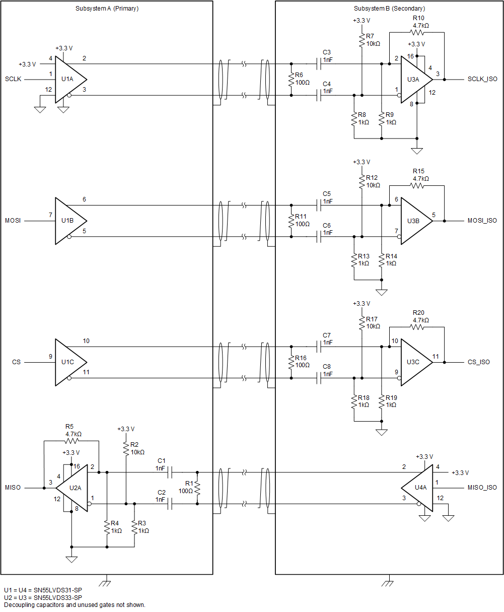
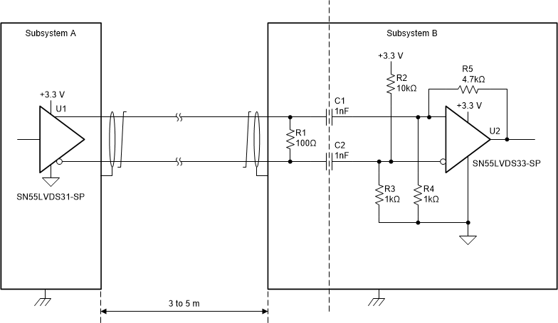
The Serial Peripheral Interface (SPI) is commonly used in embedded systems to connect microcontrollers to peripheral devices such as ADCs and DACs. It is often used in spacecraft applications, and sometimes an isolated SPI implementation is necessary to preserve the spacecraft grounding principles or to support DC offsets. The following circuit uses the SN55LVDS31-SP and SN55LVDS33-SP RS-422 driver and receiver devices to implement one channel of an isolated SPI. Isolation is provided by the AC-coupling capacitors, whose voltage rating determines the level of isolation supported.
The following image is a typical four-signal SPI implementation. The circuit shown uses the SN55LVDS31-SP and SN55LVDS33-SP devices and a 3.3-V supply voltage.
The circuit biases the negative input of each receiver channel slightly above ground. Positive feedback changes the bias point of the positive input depending on the output state of the receiver. When the output is high, the positive input is biased higher than the negative input; when the output is low, the positive input is biased lower than the negative input. In this way, the receiver always remains in the last state that it was actively driven to. The time constant of the AC-coupling circuit is irrelevant, and there is no minimum operating frequency.
Differential Inputs | Enables | Outputs | |
---|---|---|---|
VID = V(A) – V(B) | G | G | Y |
VID ≥ 50 mV | H | X | H |
X | L | H | |
VID ≤ –50 mV | H | X | L |
X | L | L | |
X | L | H | Z |
Isolation is provided by the AC-coupling capacitors. These should be chosen with a voltage rating greater than the isolation voltage required. For improved failure tolerance, two capacitors in series can be used; however, each capacitor must be rated for the full isolation voltage.
In the following description the component reference designators referred to are those used in the circuit diagram on the first page of this document.
This yields the following equation for the differential input voltage:
Therefore, the following equation shows the differential input voltage:
The time constant of C1, R4, and R5 is given in the following equation: