-
LM2742 Buck Controller Evaluation Module User's Guide
LM2742 Buck Controller Evaluation Module User's Guide
Trademarks
All trademarks are the property of their respective owners.
1 Specifications of the Board
The LM2742 Evaluation board has been designed for a wide variety of components in order to show the flexibility of the LM2742 IC. The example design steps input voltages from 2.0 V to 13.2 V, down to 1.2 V, at 4 A, with a switching frequency of 500 kHz. This design can be modified by following the Design Considerations section of the LM2742 N-Channel FET Synchronous Buck Regulator Controller for Low Output Voltagesd ata sheet. The board is four layers, consisting of signal/power traces on top and bottom, one internal ground plane, and an internal split power plane. All planes are 1-oz. copper, and the board is 62-mil FR4 laminate.
2 MOSFET Footprints
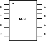
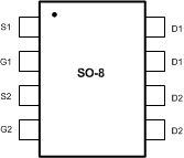
The LM2742 demo board has three footprints for single N-MOSFETs with SO-8 packages and standard pinouts. See Figure 2-1. Q1 is the high-side FET. Q2 and Q3 are connected in parallel for the low-side FET to accommodate higher currents when the circuit design uses low duty cycles. Q4 is a footprint for a dual N-MOSFET in SO-8 with a pinout shown in Figure 2-2.
 Figure 2-1 Single N-MOSFETs with SO-8
Package
 Figure 2-2 Dual N-MOSFETs with SO-8
Package