How to Prevent Battery over Discharge by Using a Precise Threshold Voltage Enable Pin
Using a buck-boost converter is a convenient way to obtain a fixed supply voltage within the wide voltage range of typical batteries used in low-power devices such as smart meters, wearables or those in the Internet of Things. In order to extract as much energy as possible from the battery, it helps if the converter can operate at very low input voltages.
In buck-boost devices such as the TPS63802, the minimum operating input voltage is as low as 1.3 V once the device is started. With most rechargeable batteries, however, deep discharge can irreversibly damage the battery. In such situations, it becomes useful to have the option to cut off the battery supply at a desired value, say 2.5 V for a one-cell lithium-ion battery.
A typical DC/DC converter has an input pin to enable or disable the converter. However, the threshold voltage at this pin usually has a high tolerance, making it difficult to pinpoint the desired cutoff voltage. As an example, according to its data sheet, the threshold voltage of the enable (EN) pin for the TPS63020 is somewhere within the range listed in Table 1.
| Parameter | Min | Typ | Max | Unit | |
|---|---|---|---|---|---|
| VIL | EN input low voltage | 0.4 | V | ||
| VIH | EN input high voltage | 1.2 | V | ||
This threshold range is fine for on/off control using logic-level signals, but not if you want to set a precise cutoff voltage derived from the input voltage. To achieve higher accuracy, it is possible to add a comparator and a voltage reference, but this increases complexity and cost.
My colleague Chris Glaser introduced the concept of achieving a precise threshold voltage for buck converters in his Analog Design Journal article, “Achieving a clean startup by using a DC/DC converter with a precise enable-pin threshold.” The new TPS63802 buck-boost converter also has very precise threshold voltage for the EN pin, with approximately 3% accuracy and 100-mV hysteresis, as listed in Table 2.
| Parameter | Min | Typ | Max | Unit | |
|---|---|---|---|---|---|
| VTHR,EN | Rising threshold voltage for EN pin | 1.07 | 1.1 | 1.13 | V |
| VTHF,EN | Falling threshold voltage for EN pin | 0.97 | 1 | 1.03 | V |
It is possible to easily set a user-defined minimum supply voltage with a voltage divider, as shown in Figure 1.
 Figure 1 Setting the input cutoff
voltage with a voltage divider
Figure 1 Setting the input cutoff
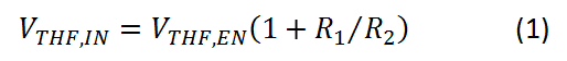
voltage with a voltage dividerEquation 1 expresses the falling threshold supply voltage when the converter is turned off as:
Equation 2 calculates the rising threshold supply voltage when the converter is turned on:

The additional voltage divider will increase the current consumption; therefore, aim for large resistances. However, considering that the EN input leakage current is 0.2 μA maximum, aim for at least 20 μA of current in the voltage divider. The application report, “Optimizing Resistor Dividers at a Comparator Input,” has more details about how to optimize a resistor divider at a comparator input.
As an example, to set the cutoff input voltage to VTHF,IN = 2.5 V, first choose R1 + R2 = 125 kΩ to have a 20-μA resistor divider current. Solving Equation 1, choose R1 = 75 kΩ and R2 = 49.9 kΩ resistors with 1% tolerance. The turn-on input voltage is now VTHF,IN = 2.75 V according to Equation 2.
Figure 2 shows that the achieved cutoff and turn-on input voltages are 2.56 V and 2.8 V, respectively. This is within the equivalent 6σ tolerance of approximately 80 mV (3.1%) caused by the EN pin threshold voltage and resistor tolerances, not taking into account oscilloscope accuracy. The application report, “AN-1378 Method for Calculating Output Voltage Tolerances in Adjustable Regulators,” has more details on calculating equivalent voltage tolerances.
 Figure 2 Achieved Cutoff and Turn-on
Input Voltage Thresholds
Figure 2 Achieved Cutoff and Turn-on
Input Voltage ThresholdsConclusion
The previous example showed how you can easily protect your battery from overdischarge by adding only 2 resistors. The same solution is applicable not only to buck-boost but also to other buck or boost devices with a precise EN pin threshold voltage.
If you have any questions about TI buck-boost devices, see the TI E2E™ Community Power Management forum.
IMPORTANT NOTICE AND DISCLAIMER
TI PROVIDES TECHNICAL AND RELIABILITY DATA (INCLUDING DATASHEETS), DESIGN RESOURCES (INCLUDING REFERENCE DESIGNS), APPLICATION OR OTHER DESIGN ADVICE, WEB TOOLS, SAFETY INFORMATION, AND OTHER RESOURCES “AS IS” AND WITH ALL FAULTS, AND DISCLAIMS ALL WARRANTIES, EXPRESS AND IMPLIED, INCLUDING WITHOUT LIMITATION ANY IMPLIED WARRANTIES OF MERCHANTABILITY, FITNESS FOR A PARTICULAR PURPOSE OR NON-INFRINGEMENT OF THIRD PARTY INTELLECTUAL PROPERTY RIGHTS.
These resources are intended for skilled developers designing with TI products. You are solely responsible for (1) selecting the appropriate TI products for your application, (2) designing, validating and testing your application, and (3) ensuring your application meets applicable standards, and any other safety, security, or other requirements. These resources are subject to change without notice. TI grants you permission to use these resources only for development of an application that uses the TI products described in the resource. Other reproduction and display of these resources is prohibited. No license is granted to any other TI intellectual property right or to any third party intellectual property right. TI disclaims responsibility for, and you will fully indemnify TI and its representatives against, any claims, damages, costs, losses, and liabilities arising out of your use of these resources.
TI’s products are provided subject to TI’s Terms of Sale (www.ti.com/legal/termsofsale.html) or other applicable terms available either on ti.com or provided in conjunction with such TI products. TI’s provision of these resources does not expand or otherwise alter TI’s applicable warranties or warranty disclaimers for TI products.
Mailing Address: Texas Instruments, Post Office Box 655303, Dallas, Texas 75265
Copyright © 2023, Texas Instruments Incorporated