-
A Bite-Size Gate Drive: Replacing BJTs With an Integrated Solution
A Bite-Size Gate Drive: Replacing BJTs With an Integrated Solution
Jonathan Kanter
Sushi is wonderful. It packs a fresh, satisfying flavor into a small package that melds the subtleties of just a few ingredients to make something special. It reminds me of the ideal power supply: a small, efficient collection of stages that produces the power to drive your amazing product.
In this analogy, the power factor correction (PFC) stage is like the rice in good sushi. Just as rice creates a base that enables other ingredients to shine, the PFC stage makes it possible for other components to deliver power to the end product. The responsiveness of the metal-oxide semiconductor field-effect transistor (MOSFET) to the changes in output signal from the PFC controller is crucial to the PFC stage. For the timing to be correct, the gate-drive circuit must switch the FET only when it’s supposed to.
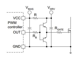
The application report “Fundamentals of MOSFET and IGBT Gate Driver Circuits” details a number of methods to effectively drive MOSFET gates, including the popular bipolar totem-pole pictured in Figure 1.
 Figure 1 Bipolar Junction Transistor
(BJT) Totem-Pole Gate-drive Circuit
Figure 1 Bipolar Junction Transistor
(BJT) Totem-Pole Gate-drive CircuitYou can use the configuration in Figure 1 to effectively drive 3A to 6A to the MOSFET gate, but there are a couple of drawbacks that a gate-driver integrated circuit (IC) can rectify related to board space, system design complexity, noise immunity and thermal protection.
Board Space and System Design Complexity
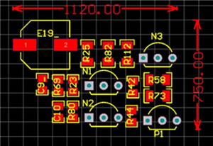
One common place where you need a gate-drive circuit is in the PFC stage. In the example layout of a PFC solution with a level shift shown in Figure 2, the design requires 17 discrete components and 0.84in2 (or 542mm2) of printed circuit board (PCB) space.
 Figure 2 PFC Solution With Only
Discrete Components
Figure 2 PFC Solution With Only
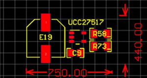
Discrete ComponentsThe same design using a gate-driver IC (Figure 3) such as the UCC27517 to drive the MOSFET gate requires only five total components and occupies only 0.33in2 (or 212mm2) of PCB space.
 Figure 3 PFC Solution Using the
UCC27517 MOSFET Gate Driver
Figure 3 PFC Solution Using the
UCC27517 MOSFET Gate DriverIn addition to the decrease in board space, the decrease in discrete components enables you to spend less time and effort to ensure proper switch timing.
Noise Immunity
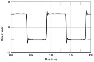
In a perfect world, the gate-drive output of your PFC controller would be a perfect square wave. But due to the parasitic components present in every PFC design, there is almost always noise introduced upon switching, causing the generated wave to look like Figure 4.
 Figure 4 Example PFC Controller Output
Waveform
Figure 4 Example PFC Controller Output
WaveformNotice the oscillation in the signal when the logic level switches, which can be much larger than what you see in Figure 4. In order to design the most efficient PFC circuit possible, you want your MOSFET to only switch when you want it to so as to ultimately output the smoothest possible sinusoidal current waveform. Therefore, it is important for your gate-drive circuit to have a large-enough input hysteresis (the difference between the input signal high threshold and low threshold) so that the MOSFET does not switch when this noise occurs.
In the discrete solution, current will be driven to the MOSFET gate if the input voltage is greater than 0.7V, meaning that the hysteresis is very small. In contrast, integrated driver ICs will not switch output logic levels unless the input voltage reaches a value significantly below or above the high and low logic input levels, respectively, thus protecting your system from the negative effects of input noise.
Thermal Protection
Smooth power up and power down can sometimes be forgotten when designing a power supply, but both are vital to a system’s long-term health. When using a discrete solution, the gate-drive output can occur at any time, even if the voltage driven to the gate is not high enough. When a high current is driven to a FET gate without accompanying voltage, an excessive amount of power dissipates across the FET, which leads to overheating and potentially damage.
In contrast, many low-side gate-driver ICs have an undervoltage lockout (UVLO) protection feature, meaning that the gate-drive output is disabled until it is supplied with the necessary voltage, which protects your system from thermal damage. For more details on this subject, check out the application note, Low-Side Gate Drivers With UVLO Versus BJT Totem-Pole.
Becoming a head sushi chef (or itamae) takes years of training, and although it may not seem like the most important part of the craft, the ability to make rice that has the ideal form and consistency to create quality sushi is vital to attaining this status. Much like the time and effort that itamaes put into rice, gate-driver IC designers spend many hours making a quality device for driving a MOSFET gate.
With that in mind, consider the performance advantages that gate-driver ICs have over their discrete counterparts when choosing the design of your solution. For more information on how to choose a gate driver for your design, check out the TI Training “Know Your Gate Driver” video series.
Additional Resources
- Check out TI’s MOSFET and insulated gate bipolar transistor (IGBT) gate drivers.
- Find in-depth training on all things high voltage in the “High Volt Interactive Training Series.”
- Read these Power House blog posts:
IMPORTANT NOTICE AND DISCLAIMER
TI PROVIDES TECHNICAL AND RELIABILITY DATA (INCLUDING DATASHEETS), DESIGN RESOURCES (INCLUDING REFERENCE DESIGNS), APPLICATION OR OTHER DESIGN ADVICE, WEB TOOLS, SAFETY INFORMATION, AND OTHER RESOURCES “AS IS” AND WITH ALL FAULTS, AND DISCLAIMS ALL WARRANTIES, EXPRESS AND IMPLIED, INCLUDING WITHOUT LIMITATION ANY IMPLIED WARRANTIES OF MERCHANTABILITY, FITNESS FOR A PARTICULAR PURPOSE OR NON-INFRINGEMENT OF THIRD PARTY INTELLECTUAL PROPERTY RIGHTS.
These resources are intended for skilled developers designing with TI products. You are solely responsible for (1) selecting the appropriate TI products for your application, (2) designing, validating and testing your application, and (3) ensuring your application meets applicable standards, and any other safety, security, or other requirements. These resources are subject to change without notice. TI grants you permission to use these resources only for development of an application that uses the TI products described in the resource. Other reproduction and display of these resources is prohibited. No license is granted to any other TI intellectual property right or to any third party intellectual property right. TI disclaims responsibility for, and you will fully indemnify TI and its representatives against, any claims, damages, costs, losses, and liabilities arising out of your use of these resources.
TI’s products are provided subject to TI’s Terms of Sale (www.ti.com/legal/termsofsale.html) or other applicable terms available either on ti.com or provided in conjunction with such TI products. TI’s provision of these resources does not expand or otherwise alter TI’s applicable warranties or warranty disclaimers for TI products.
Mailing Address: Texas Instruments, Post Office Box 655303, Dallas, Texas 75265
Copyright © 2023, Texas Instruments Incorporated