Flyback Converters: Two Outputs Are Better than One
David Strasser
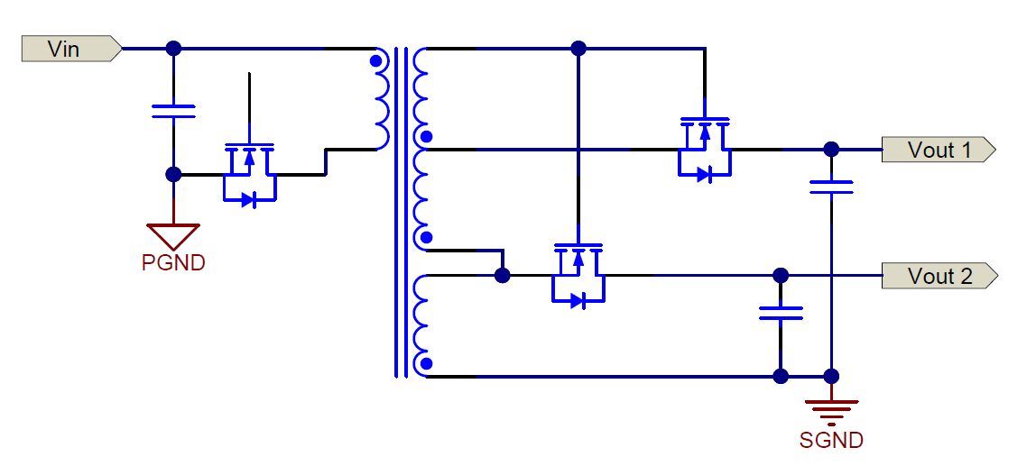
Flyback converters are widely used for applications that require isolation between the primary and secondary. The flyback converter’s single primary switch and output rectifier provide a cost effective solution for a single output. Often times, more than one output voltage is required. Typically the flyback converter generates an isolated output, say 5V, and a point-of-load (POL) nonisolated converter generates a second output, such as 3.3V, from the 5V output (Figure 1). An input capacitor and output inductor, as a minimum, are required if the POL IC has internal FETs. A more cost effective alternative is to add a second winding to the flyback transformer plus a second rectifier to generate the second output (Figure 2). The second winding plus rectifier add only a few cents to the cost of the design versus the POL IC, input capacitor and inductor.
 Figure 1 Single Isolated Output with
POL Converter for Second Output
 Figure 2 Dual Isolated Outputs with
Extra Transformer Winding/rectifier
Figure 2 Dual Isolated Outputs with
Extra Transformer Winding/rectifierOne of the outputs is typically regulated by the feedback control loop while the other output tracks the regulated output through the transformer turns ratio. Synchronous rectification is usually implemented on the outputs, minimizing the voltage drop variation across the rectifiers over load and providing good cross-regulation. Minimizing the transformer leakage inductance is also critical for good cross-regulation.
There are two methods used to drive the synchronous rectifiers. The first and most simple way is to add a gate drive winding to the flyback power transformer (Figure 3). This is known as the “self-driven” technique and only adds a few cents to the cost of the transformer. There is little control of the timing between the primary FET and synchronous FET switching, which is a drawback. There will be a short time period when the primary FET and synchronous FET are both on, creating a short which will result in shoot-through current, increased power dissipation and reduced efficiency.
 Figure 3 “Self-driven” Method to Control Synchronous FETs
A second method for driving the synchronous rectifiers is to add a separate gate drive transformer (Figure 4). The cost is higher than adding a winding on the flyback power transformer, but still less than adding a POL converter. The advantage is there is now direct control of the switching of the synchronous FETs, which will reduce shoot-through current and improve efficiency. Using a pulse width modulation (PWM) controller IC such as TI’s UCC2897A or TPS23754 with two gate drivers and adjustable delay will further reduce or eliminate the shoot-through current, resulting in even better efficiency.
 Figure 4 Separate Gate Drive Transformer to Control Synchronous FETs
Links to examples of dual output flyback converters with synchronous rectifiers are below. The first two examples use the self-driven method to control the synchronous FETs. The third example, while only a single output, demonstrates the gate drive transformer used to control the synchronous FET and the PWM controller IC with dual gate drivers/adjustable delay. Figure 4 shows how this can be extended to dual outputs.
- TI Designs Class 3 Dual Output Isolated Flyback Converter for PoE Applications Reference Design is an isolated Type 1 Power over Ethernet (PoE) flyback converter with dual 5V/3.3V outputs. It uses the TPS23753A Powered Device (PD)/PWM controller with a single gate drive. Self-driven synchronous rectification provides very good efficiency and cross-regulation between the outputs.
- High Efficiency 36-60V Input Isolated Synchronous Flyback Reference Design with Dual Outputs is an isolated flyback converter for telecom applications with dual 5V/3.3V outputs at 22W. It uses the LM5020 PWM controller with a single gate drive. Self-driven synchronous rectification provides very good efficiency and cross-regulation between the outputs.
- Class 4, Efficiency-Optimized Flyback Converter for PoE Applications is an isolated Type 4 PoE flyback converter. It only has a single 5V output, but uses both the separate gate-drive transformer and the TPS23754 PD/PWM controller with dual gate drives. The converter-only efficiency is 92%.
If one of these designs does not meet your needs, you can search the TI Designs power reference library. It contains over 1,000 power converter designs for a wide variety of applications.