-
Waveform Audit: My Boost Converter Has an Off-ramp!
Waveform Audit: My Boost Converter Has an Off-ramp!
As an applications engineer, I often get inquiries about voltage and current flows in switching regulators. And I often realize that the basic theory I learned in college doesn’t always tell the whole story. A recent case with the asynchronous boost converter in the TPS65150 LCD bias device is a good example of what I mean.
Let’s start with the basic theory of how the switching node of a boost converter should look. Figure 1 shows the basic structure of an asynchronous boost converter.
 Figure 1 Simplified Boost Converter
Block Diagram
Figure 1 Simplified Boost Converter
Block DiagramWhen transistor Q1 turns on, the switch node pulls to ground and inductor L1 charges. The voltage on the switch node is approximately equal to 0V during the on time. During the off time, Q1 turns off, L1 discharges to the output, and the voltage on the switch node equals the output voltage (VO) plus the forward voltage (VF) across diode D1.
Figure 2 shows the switch-node waveform under typical operating conditions. As expected, the voltage on the switch node is rectangular and alternates between ground and VO + VF.
 Figure 2 Switch-node Waveform
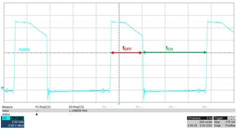
But under low-output current conditions, the switch-node waveform shape changes and looks like Figure 3. At the start of the off time the switch-node voltage is VO + VF (as before), but then it ramps down linearly. What’s causing this behavior and what’s the difference to the basic theory?
 Figure 3 Switch-node Waveform at
Low-output Currents
Figure 3 Switch-node Waveform at
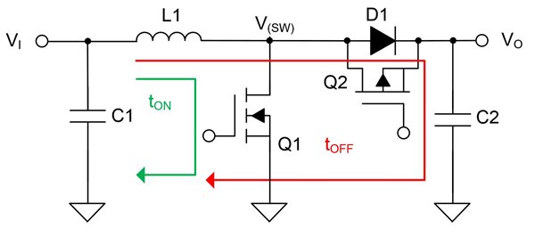
Low-output CurrentsThe internal block diagram shown in Figure 4 reveals the reason for the sloping waveform: an additional PMOS transistor (Q2) connected across the diode rectifier. This transistor is a synchronous rectifier that lets the converter operate in continuous conduction mode (CCM) under all operating conditions. It is on when the inductor current is negative and off at all other times. Because it is not the main rectifier, the Rds(on) of Q2 can be relatively high (a few ohms) without decreasing efficiency much, but the high Rds(on) causes a voltage drop on the switch node when the negative inductor current flows through it. And because the inductor current is linearly increasing, the voltage drop also increases, causing the slope shown in Figure 3.
 Figure 4 Internal Block Diagram Showing
Synchronous Rectifier
Figure 4 Internal Block Diagram Showing
Synchronous RectifierFigure 5 shows the inductor current as well as the switch-node voltage and confirms that the ramp on the switch-node voltage starts when the inductor current goes negative, and increases as the inductor current increases.
 Figure 5 Switch-node Voltage and
Inductor-current Waveforms
Figure 5 Switch-node Voltage and
Inductor-current WaveformsBe aware that the ramp starts for all output currents below the critical conduction point. You can calculate the critical conduction current with Equation Figure 1:
 Figure 6 (1)
where D is the duty cycle (boost:
 ), L is the inductance and is the
switching frequency.
If you want get a deeper understanding of voltage and current flows in switching regulators, download the tool, “Power Stage Designer of Most Commonly Used Switch-Mode Power Supplies.
If you have experienced similar waveforms in your power-supply design of power supplies that you cannot explain – but would like to know the reason for, – just add a comment below.
Additional Resources:
IMPORTANT NOTICE AND DISCLAIMER
TI PROVIDES TECHNICAL AND RELIABILITY DATA (INCLUDING DATASHEETS), DESIGN RESOURCES (INCLUDING REFERENCE DESIGNS), APPLICATION OR OTHER DESIGN ADVICE, WEB TOOLS, SAFETY INFORMATION, AND OTHER RESOURCES “AS IS” AND WITH ALL FAULTS, AND DISCLAIMS ALL WARRANTIES, EXPRESS AND IMPLIED, INCLUDING WITHOUT LIMITATION ANY IMPLIED WARRANTIES OF MERCHANTABILITY, FITNESS FOR A PARTICULAR PURPOSE OR NON-INFRINGEMENT OF THIRD PARTY INTELLECTUAL PROPERTY RIGHTS.
These resources are intended for skilled developers designing with TI products. You are solely responsible for (1) selecting the appropriate TI products for your application, (2) designing, validating and testing your application, and (3) ensuring your application meets applicable standards, and any other safety, security, or other requirements. These resources are subject to change without notice. TI grants you permission to use these resources only for development of an application that uses the TI products described in the resource. Other reproduction and display of these resources is prohibited. No license is granted to any other TI intellectual property right or to any third party intellectual property right. TI disclaims responsibility for, and you will fully indemnify TI and its representatives against, any claims, damages, costs, losses, and liabilities arising out of your use of these resources.
TI’s products are provided subject to TI’s Terms of Sale (www.ti.com/legal/termsofsale.html) or other applicable terms available either on ti.com or provided in conjunction with such TI products. TI’s provision of these resources does not expand or otherwise alter TI’s applicable warranties or warranty disclaimers for TI products.
Mailing Address: Texas Instruments, Post Office Box 655303, Dallas, Texas 75265
Copyright © 2023, Texas Instruments Incorporated