-
LM3150 Wide-VIN Synchronous Buck Controller
- 1 Features
- 2 Applications
- 3 Description
- 4 Typical Application Schematic
- 5 Revision History
- 6 Pin Configuration and Functions
- 7 Specifications
- 8 Detailed Description
- 9 Application and Implementation
- 10Power Supply Recommendations
- 11Layout
- 12Device and Documentation Support
- 13Mechanical, Packaging, and Orderable Information
- IMPORTANT NOTICE
Package Options
Mechanical Data (Package|Pins)
- PWP|14
Thermal pad, mechanical data (Package|Pins)
- PWP|14
Orderable Information
LM3150 Wide-VIN Synchronous Buck Controller
1 Features
- PowerWise™ Step-Down Controller
- 6-V to 42-V Wide Input Voltage Range
- Adjustable Output Voltage Down to 0.6 V
- Programmable Switching Frequency up to 1 MHz
- No Loop Compensation Required
- Fully WEBENCH® Enabled
- Low External Component Count
- Constant On-Time (COT) Control
- Ultra-Fast Transient Response
- Stable With Low ESR Capacitors
- Output Voltage PreBias Startup
- Valley Current Limit
- Programmable Soft-Start
- Create a Custom Design Using the LM3150 with the WEBENCH Power Designer
2 Applications
- Telecom
- Networking Equipment
- Routers
- Security Surveillance
- Power Modules
3 Description
The LM3150 SIMPLE SWITCHER® controller is an easy-to-use and simplified step-down power controller capable of providing up to 12 A of output current in a typical application. Operating with an input voltage range of 6 V to 42 V, the LM3150 controller features an adjustable output voltage down to 0.6 V. The switching frequency is adjustable up to 1 MHz and the synchronous architecture provides for highly efficient designs. The LM3150 controller employs a constant on-time (COT) architecture with a proprietary emulated ripple mode (ERM) control that allows for the use of low ESR output capacitors, which reduces overall solution size and output voltage ripple. The COT regulation architecture allows for fast transient response and requires no loop compensation, which reduces external component count and reduces design complexity.
Fault protection features such as thermal shutdown, undervoltage lockout, overvoltage protection, short-circuit protection, current limit, and output voltage prebias start-up allow for a reliable and robust solution.
The LM3150 concept provides for an easy-to-use complete design using a minimum number of external components and TI’s WEBENCH online design tool. WEBENCH provides design support for every step of the design process and includes features such as external component calculation with a new MOSFET selector, electrical simulation, thermal simulation, and Build-It boards for prototyping.
Device Information(1)
| PART NUMBER | PACKAGE | BODY SIZE (NOM) |
|---|---|---|
| LM3150 | HTSSOP (14) | 5.00 mm × 4.40 mm |
- For all available packages, see the orderable addendum at the end of the datasheet.
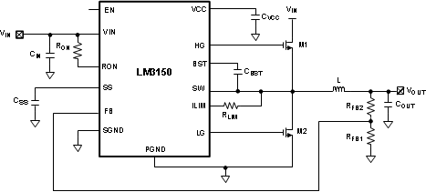
4 Typical Application Schematic

5 Revision History
Changes from F Revision (December 2014) to G Revision
- Changed graphic Inductor Current to Current Limit section. Go
Changes from E Revision (November 2012) to F Revision
- Added ESD Ratings table, Feature Description section, Device Functional Modes, Application and Implementation section, Power Supply Recommendations section, Layout section, Device and Documentation Support section, and Mechanical, Packaging, and Orderable Information section Go
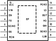
6 Pin Configuration and Functions

Pin Functions
| PIN | I/O | DESCRIPTION | FUNCTION | |
|---|---|---|---|---|
| NAME | NO. | |||
| VCC | 1 | O | Supply Voltage for FET Drivers | Nominally regulated to 5.95 V. Connect a 1.0-µF to 4.7-µF decoupling capacitor from this pin to ground. |
| VIN | 2 | I | Input Supply Voltage | Supply pin to the device. Nominal input range is 6 V to 42 V. |
| EN | 3 | I | Enable | To enable the IC, apply a logic high signal to this pin greater than 1.26-V typical or leave floating. To disable the part, ground the EN pin. |
| FB | 4 | I | Feedback | Internally connected to the regulation, overvoltage, and short-circuit comparators. The regulation setting is 0.6 V at this pin. Connect to feedback resistor divider between the output and ground to set the output voltage. |
| SGND | 5,9 | — | Signal Ground | Ground for all internal bias and reference circuitry. Should be connected to PGND at a single point. |
| SS | 6 | I | Soft-Start | An internal 7.7-µA current source charges an external capacitor to provide the soft-start function. |
| RON | 7 | I | On-time Control | An external resistor from VIN to this pin sets the high-side switch on-time. |
| ILIM | 8 | I | Current Limit | Monitors current through the low-side switch and triggers current limit operation if the inductor valley current exceeds a user defined value that is set by RLIM and the Sense current, ILIM-TH, sourced out of this pin during operation. |
| SW | 10 | O | Switch Node | Switch pin of controller and high-gate driver lower supply rail. A boost capacitor is also connected between this pin and BST pin |
| HG | 11 | O | High-Side Gate Drive | Gate drive signal to the high-side NMOS switch. The high-side gate driver voltage is supplied by the differential voltage between the BST pin and SW pin. |
| BST | 12 | I | Connection for Bootstrap Capacitor | High-gate driver upper supply rail. Connect a 0.33 to 0.47-µF capacitor from SW pin to this pin. An internal diode charges the capacitor during the high-side switch off-time. Do not connect to an external supply rail. |
| LG | 13 | O | Low-Side Gate Drive | Gate drive signal to the low-side NMOS switch. The low-side gate driver voltage is supplied by VCC. |
| PGND | 14 | G | Power Ground | Synchronous rectifier MOSFET source connection. Tie to power ground plane. Should be tied to SGND at a single point. |
| EP | — | — | Exposed Pad | Exposed die attach pad should be connected directly to SGND. Also used to help dissipate heat out of the IC. |