SNVSA29 May 2015 LM36922
PRODUCTION DATA.
- 1 Features
- 2 Applications
- 3 Description
- 4 Revision History
- 5 Pin Configuration and Functions
- 6 Specifications
-
7 Detailed Description
- 7.1 Overview
- 7.2 Functional Block Diagram
- 7.3 Feature Description
- 7.4
Device Functional Modes
- 7.4.1 Brightness Control Modes
- 7.4.2 Boost Switching Frequency
- 7.4.3 Auto Switching Frequency
- 7.4.4 Backlight Adjust Input (BL_ADJ)
- 7.4.5
Fault Protection/Detection
- 7.4.5.1
Overvoltage Protection (OVP)
- 7.4.5.1.1 Case 1 OVP Fault Only (OVP Threshold Hit and All Enabled Current Sink Inputs > 40 mV)
- 7.4.5.1.2 Case 2a OVP Fault and Open LED String Fault (OVP Threshold Occurrence and Any Enabled Current Sink Input ≤ 40 mV)
- 7.4.5.1.3 Case 2b OVP Fault and Open LED String Fault (OVP Threshold Duration and Any Enabled Current Sink Input ≤ 40 mV)
- 7.4.5.1.4 OVP/LED Open Fault Shutdown
- 7.4.5.1.5 Testing for LED String Open
- 7.4.5.2 LED String Short Fault
- 7.4.5.3 Overcurrent Protection (OCP)
- 7.4.5.4 Device Overtemperature (TSD)
- 7.4.5.1
Overvoltage Protection (OVP)
- 7.5 Programming
- 7.6 Register Maps
- 8 Applications and Implementation
- 9 Power Supply Recommendations
- 10Layout
- 11Device and Documentation Support
- 12Mechanical, Packaging, and Orderable Information
Package Options
Mechanical Data (Package|Pins)
- YFF|12
Thermal pad, mechanical data (Package|Pins)
Orderable Information
1 Features
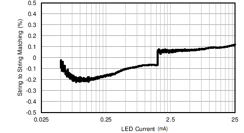
- 1% Matched Current Sinks Across (Process, Voltage, Temp)
- 3% Current Sink Accuracy Across (Process, Voltage, Temp)
- 11-Bit Dimming Resolution
- Up to 91.6% Solution Efficiency
- Drives from One to Two Parallel LED Strings at up to 28 V
- PWM Dimming Input
- I2C Programmable
- Selectable 500-kHz and 1-MHz Switching Frequency with Optional –12% shift
- Auto Switch Frequency Mode (250 kHz, 500 kHz, 1 MHz)
- Four Configurable Overvoltage Protection Thresholds (17 V, 21 V, 25 V, 29 V)
- Four Configurable Overcurrent Protection Thresholds (750 mA, 1000 mA, 1250 mA, 1500 mA)
- Thermal Shutdown Protection
2 Applications
Power Source for Smart Phone and Tablet Backlighting
3 Description
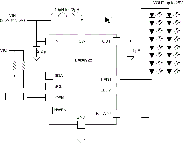
The LM36922 is an ultra-compact, highly efficient, two string white-LED driver designed for LCD display backlighting. The device can power up to 8 series LEDs at up to 25 mA per string. An adaptive current regulation method allows for different LED voltages in each string while maintaining current regulation.
The LED current is adjusted via an I2C interface or through a logic level PWM input. The PWM duty cycle is internally sensed and mapped to an 11-bit current thus allowing for a wide range of PWM frequencies and noise-free operation.
The device operates over the 2.5-V to 5.5-V input voltage range and -40°C to 85°C temperature range.
Device Information(1)
| PART NUMBER | PACKAGE | BODY SIZE (MAX) |
|---|---|---|
| LM36922 | DSBGA (12) | 1.755 mm x 1.355 mm |
- For all available packages, see the orderable addendum at the end of the datasheet.
space
space
space
space
space
space
Simplified Schematic

Typical String-to-String Matching vs LED Current
