LMH6654, LMH6655 Single and Dual Low Power, 250 MHz, Low Noise Amplifiers
1 Features
- (VS = ±5 V, TJ = 25 °C, Typical Values Unless Specified)
- Voltage Feedback Architecture
- Unity Gain Bandwidth 250 MHz
- Supply Voltage Range ±2.5V to ±6V
- Slew Rate 200 V/µsec
- Supply Current 4.5 mA/channel
- Input Common Mode Voltage −5.15V to +3.7V
- Output Voltage Swing (RL = 100 Ω) −3.6V to 3.4V
- Input Voltage Noise 4.5 nV/√Hz
- Input Current Noise 1.7 pA/√Hz
- Settling Time to 0.01% 25 ns
2 Applications
- ADC Drivers
- Consumer Video
- Active Filters
- Pulse Delay Circuits
- xDSL Receiver
- Pre-amps
3 Description
The LMH6654 and LMH6655 single and dual high speed voltage feedback amplifiers are designed to have unity-gain stable operation with a bandwidth of 250 MHz. They operate from ±2.5 V to ±6 V and each channel consumes only 4.5 mA. The amplifiers feature very low voltage noise and wide output swing to maximize signal-to-noise ratio, and possess a true single supply capability with input common mode voltage range extending 150 mV below negative rail and within 1.3 V of the positive rail. The high speed and low power combination of the LMH6654 and LMH6655 make these products an ideal choice for many portable, high speed applications where power is at a premium.
The LMH6654 and LMH6655 are built on TI’s Advance VIP10™ (Vertically Integrated PNP) complementary bipolar process.
The LMH6654 is packaged in 5-Pin SOT-23 and 8-Pin SOIC. The LMH6655 is packaged in 8-Pin VSSOP (DGK) and 8-Pin SOIC.
Device Information(1)
| PART NUMBER | PACKAGE | BODY SIZE (NOM) |
|---|---|---|
| LMH6654 | SOIC (8) | 4.90 mm x 3.91 mm |
| LMH6654 | SOT-23 (5) | 2.90 mm x 1.60 mm |
| LMH6655 | SOIC (8) | 4.90 mm x 3.91 mm |
| LMH6655 | VSSOP (8) | 3.00 mm x 3.00 mm |
- For all available packages, see the orderable addendum at the end of the datasheet.
3.1 Input Voltage and Curernt Noise vs. Frequency (Vs= ±5V)

4 Revision History
Changes from D Revision (March 2013) to E Revision
- Changed data sheet structure and organization. Added, updated, or renamed the following sections: Device Information Table, Application and Implementation; Power Supply Recommendations; Device and Documentation Support; Mechanical, Packaging, and Ordering Information. Deleted Switching Characteristics due to redundancy. Go
- Changed from Junction Temperature Range to "Operating Temperature Range"Go
- Deleted TJ = 25°CGo
- Deleted TJ = 25°C Go
Changes from C Revision (March 2013) to D Revision
- Changed layout of National Data Sheet to TI formatGo
5 Pin Configuration and Functions


Pin Functions
| PIN | I/O | DESCRIPTION | ||||
|---|---|---|---|---|---|---|
| NAME | LMH6654 | LMH6655 | ||||
| DBV | D | DGK | ||||
| -IN | 4 | 2 | I | Inverting Input | ||
| +IN | 3 | 3 | I | Non-inverting Input | ||
| -IN A | 2 | I | ChA Inverting Input | |||
| +IN A | 3 | I | ChA Non-inverting Input | |||
| -IN B | 6 | I | ChB Inverting Input | |||
| +IN B | 5 | I | ChB Non-inverting Input | |||
| N/C | 1, 5, 8 | –– | No Connection | |||
| OUT A | 1 | O | ChA Output | |||
| OUT B | 7 | O | ChB Output | |||
| OUTPUT | 1 | 6 | O | Output | ||
| V- | 2 | 4 | 4 | I | Negative Supply | |
| V+ | 5 | 7 | 8 | I | Positive Supply | |
6 Specifications
6.1 Absolute Maximum Ratings
over operating free-air temperature range (unless otherwise noted)(1)| MIN | MAX | UNIT | ||
|---|---|---|---|---|
| VIN Differential | ±1.2 | V | ||
| Output Short Circuit Duration | See (3) | |||
| Supply Voltage (V+ − V−) | 13.2 | V | ||
| Voltage at Input pins | V+ +0.5 V- -0.5 |
V | ||
| Junction Temperature(4) | 150 | °C | ||
| Soldering Information | Infrared or Convection (20 sec.) | 235 | °C | |
| Wave Soldering (10 sec.) | 260 | °C | ||
6.2 Handling Ratings
| MIN | MAX | UNIT | |||
|---|---|---|---|---|---|
| Tstg | Storage temperature range | −65 | 150 | °C | |
| V(ESD) | Electrostatic discharge(2) | Human body model (HBM), per ANSI/ESDA/JEDEC JS-001, all pins(1) |
2000 | V | |
| Machine model (MM)(2) | 200 | ||||
6.3 Recommended Operating Conditions(1)
over operating free-air temperature range (unless otherwise noted)| MIN | NOM | MAX | UNIT | ||
|---|---|---|---|---|---|
| Supply Voltage (V+ - V−) | ±2.5 | ±6.0 | V | ||
| Operating Temperature Range | −40 | 85 | °C | ||
6.4 Thermal Information
| THERMAL METRIC(1) | SOIC (D) | VSSOP (DGK) | SOT-23 (D) | UNIT | |
|---|---|---|---|---|---|
| 8 PINS | 8 PINS | 5 PINS | |||
| RθJA | Junction-to-ambient thermal resistance | 172 | 235 | 265 | °C/W |
±5V Electrical Characteristics
Unless otherwise specified, all limits ensured for V+ = +5V, V− = −5V, VCM = 0V, AV = +1, RF = 25Ω for gain = +1, RF = 402Ω for gain ≥ +2, and RL = 100Ω. Boldface limits apply at the temperature extremes.| PARAMETER | TEST CONDITIONS | MIN(6) | TYP(5) | MAX(6) | UNIT | |
|---|---|---|---|---|---|---|
| DYNAMIC PERFORMANCE | ||||||
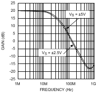
| fCL | Close Loop Bandwidth | AV = +1 | 250 | MHz | ||
| AV = +2 | 130 | |||||
| AV = +5 | 52 | |||||
| AV = +10 | 26 | |||||
| GBWP | Gain Bandwidth Product | AV ≥ +5 | 260 | MHz | ||
| Bandwidth for 0.1 dB Flatness | AV +1 | 18 | MHz | |||
| φm | Phase Margin | 50 | deg | |||
| SR | Slew Rate (8) | AV = +1, VIN = 2 VPP | 200 | V/µs | ||
| tS | Settling Time 0.01% |
AV = +1, 2V Step | 25 | ns | ||
| 0.1% | 15 | ns | ||||
| tr | Rise Time | AV = +1, 0.2V Step | 1.4 | ns | ||
| tf | Fall Time | AV = +1, 0.2V Step | 1.2 | ns | ||
| DISTORTION and NOISE RESPONSE | ||||||
| en | Input Referred Voltage Noise | f ≥ 0.1 MHz | 4.5 | nV/√Hz | ||
| in | Input-Referred Current Noise | f ≥ 0.1 MHz | 1.7 | pA/√Hz | ||
| Second Harmonic Distortion | AV = +1, f = 5 MHz | −80 | dBc | |||
| Third Harmonic Distortion | VO = 2 VPP, RL = 100Ω | −85 | ||||
| Xt | Crosstalk (for LMH6655 only) | Input Referred, 5 MHz, Channel-to-Channel | −80 | dB | ||
| DG | Differential Gain | AV = +2, NTSC, RL = 150Ω | 0.01% | |||
| DP | Differential Phase | AV = +2, NTSC, RL = 150Ω | 0.025 | deg | ||
| INPUT CHARACTERISTICS | ||||||
| VOS | Input Offset Voltage | VCM = 0V | −3 −4 |
±1 | 3 4 |
mV |
| TC VOS | Input Offset Average Drift | VCM = 0V (7) | 6 | µV/°C | ||
| IB | Input Bias Current | VCM = 0V | 5 | 12 18 |
µA | |
| IOS | Input Offset Current | VCM = 0V | −1 −2 |
0.3 | 1 2 |
µA |
| RIN | Input Resistance | Common Mode | 4 | MΩ | ||
| Differential Mode | 20 | kΩ | ||||
| CIN | Input Capacitance | Common Mode | 1.8 | pF | ||
| Differential Mode | 1 | |||||
| CMRR | Common Mode Rejection Ration | Input Referred, VCM = 0V to −5V |
70 68 |
90 | dB | |
| CMVR | Input Common- Mode Voltage Range | CMRR ≥ 50 dB | −5.15 | −5.0 | V | |
| 3.5 | 3.7 | |||||
| TRANSFER CHARACTERISTICS | ||||||
| AVOL | Large Signal Voltage Gain | VO = 4 VPP, RL = 100Ω | 60 58 |
67 | dB | |
| OUTPUT CHARACTERISTICS | ||||||
| VO | Output Swing High | No Load | 3.4 3.2 |
3.6 | V | |
| Output Swing Low | No Load | −3.9 | −3.7 −3.5 |
|||
| Output Swing High | RL = 100Ω | 3.2 3.0 |
3.4 | |||
| Output Swing Low | RL = 100Ω | −3.6 | −3.4 −3.2 |
|||
| ISC | Short Circuit Current (3) | Sourcing, VO = 0V ΔVIN = 200 mV |
145 130 |
280 | mA | |
| Sinking, VO = 0V ΔVIN = 200 mV |
100 80 |
185 | ||||
| IOUT | Output Current | Sourcing, VO = +3V | 80 | mA | ||
| Sinking, VO = −3V | 120 | |||||
| RO | Output Resistance | AV = +1, f <100 kHz | 0.08 | Ω | ||
| POWER SUPPLY | ||||||
| PSRR | Power Supply Rejection Ratio | Input Referred, VS = ±5V to ±6V |
60 | 76 | dB | |
| IS | Supply Current (per channel) | 4.5 | 6 7 |
mA | ||
5V Electrical Characteristics
Unless otherwise specified, all limits ensured for V+ = +5V, V− = −0V, VCM = 2.5V, AV = +1, RF = 25 Ω for gain = +1,RF = 402Ω for gain ≥ +2, and RL = 100Ω to V+/2. Boldface limits apply at the temperature extremes.
| PARAMETER | TEST CONDITIONS | MIN(6) | TYP(5) | MAX(6) | UNIT | |
|---|---|---|---|---|---|---|
| DYNAMIC PERFORMANCE | ||||||
| fCL | Close Loop Bandwidth | AV = +1 | 230 | MHz | ||
| AV = +2 | 120 | |||||
| AV = +5 | 50 | |||||
| AV = +10 | 25 | |||||
| GBWP | Gain Bandwidth Product | AV ≥ +5 | 250 | MHz | ||
| Bandwidth for 0.1 dB Flatness | AV = +1 | 17 | MHz | |||
| φm | Phase Margin | 48 | deg | |||
| SR | Slew Rate (8) | AV = +1, VIN = 2 VPP | 190 | V/µs | ||
| tS | Settling Time 0.01% |
AV = +1, 2V Step | 30 | ns | ||
| 0.1% | 20 | ns | ||||
| tr | Rise Time | AV = +1, 0.2V Step | 1.5 | ns | ||
| tf | Fall Time | AV = +1, 0.2V Step | 1.35 | ns | ||
| DISTORTION and NOISE RESPONSE | ||||||
| en | Input Referred Voltage Noise | f ≥ 0.1 MHz | 4.5 | nV/√Hz | ||
| in | Input Referred Current Noise | f ≥ 0.1 MHz | 1.7 | pA/√Hz | ||
| Second Harmonic Distortion | AV = +1, f = 5 MHz | −65 | dBc | |||
| Third Harmonic Distortion | VO = 2 VPP, RL = 100Ω | −70 | ||||
| Xt | Crosstalk (for LMH6655 only) | Input Referred, 5 MHz | −78 | dB | ||
| INPUT CHARACTERISTICS | ||||||
| VOS | Input Offset Voltage | VCM = 2.5V | −5 −6.5 |
±2 | 5 6.5 |
mV |
| TC VOS | Input Offset Average Drift | VCM = 2.5V (7) | 6 | µV/°C | ||
| IB | Input Bias Current | VCM = 2.5V | 6 | 12 18 |
µA | |
| IOS | Input Offset Current | VCM = 2.5V | −2 −3 |
0.5 | 2 3 |
µA |
| RIN | Input Resistance | Common Mode | 4 | MΩ | ||
| Differential Mode | 20 | kΩ | ||||
| CIN | Input Capacitance | Common Mode | 1.8 | pF | ||
| Differential Mode | 1 | |||||
| CMRR | Common Mode Rejection Ration | Input Referred, VCM = 0V to −2.5V |
70 68 |
90 | dB | |
| CMVR | Input Common Mode Voltage Range | CMRR ≥ 50 dB | −0.15 | 0 | V | |
| 3.5 | 3.7 | |||||
| TRANSFER CHARACTERISTICS | ||||||
| AVOL | Large Signal Voltage Gain | VO = 1.6 VPP, RL = 100Ω | 58 55 |
64 | dB | |
| OUTPUT CHARACTERISTICS | ||||||
| VO | Output Swing High | No Load | 3.6 3.4 |
3.75 | V | |
| Output Swing Low | No Load | 0.9 | 1.1 1.3 |
|||
| Output Swing High | RL = 100Ω | 3.5 3.35 |
3.70 | |||
| Output Swing Low | RL = 100Ω | 1 | 1.3 1.45 |
|||
| ISC | Short Circuit Current (3) | Sourcing , VO = 2.5V ΔVIN = 200 mV |
90 80 |
170 | mA | |
| Sinking, VO = 2.5V ΔVIN = 200 mV |
70 60 |
140 | ||||
| IOUT | Output Current | Sourcing, VO = +3.5V | 30 | mA | ||
| Sinking, VO = 1.5V | 60 | |||||
| RO | Output Resistance | AV = +1, f <100 kHz | .08 | Ω | ||
| POWER SUPPLY | ||||||
| PSRR | Power Supply Rejection Ratio | Input Referred , VS = ± 2.5V to ± 3V |
60 | 75 | dB | |
| IS | Supply Current (per channel) | 4.5 | 6 7 |
mA | ||
6.5 Typical Characteristics
25°C, V+ = ±5 V, V− = −5, RF = 25 Ω for gain = +1, RF = 402 Ω for gain ≥ +2 and RL = 100 Ω, unless otherwise specified.


vs. Supply Voltage
 Figure 7. Offset Voltage
vs. Supply Voltage (VCM = 0V)
 Figure 9. Offset Voltage
vs. Common Mode
 Figure 11. Bias Current
vs. Common Mode Voltage
 Figure 13. AOL, PSRR and CMRR
vs. Temperature
 Figure 15. Inverting Large Signal Pulse Response
(VS = ±5V)
 Figure 17. Non-Inverting Large Signal Pulse Response
 (VS = ±5V)

(VS = ±5V)

(VS = ±5V)
vs. Frequency (VS = ±5V)
 Figure 25. Harmonic Distortion
vs. Frequency
G = +1, VO = 2 VPP, VS = ±5V
 Figure 27. Harmonic Distortion
vs. Temperature
VS = ±5V, f = 5 MHz, VO = 2 VPP
 Figure 29. Harmonic Distortion
vs. Gain
VS = ±5V, f = 5 MHz, VO = 2 VPP

vs. Output Swing
(G = +2, VS = ±5V, f = 5 MHz)


 Figure 37. CrossTalk
vs. Frequency (LMH6655 only)
 Figure 39. Open Loop Gain and Phase
vs. Frequency


vs. Temperature
 Figure 8. Offset Voltage
vs. Common Mode
 Figure 10. Bias Current and Offset Voltage
vs. Temperature
 Figure 12. Bias Current
vs. Common Mode Voltage
 Figure 14. Inverting Large Signal Pulse Response
 (VS = 5V)
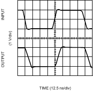 Figure 16. Non-Inverting Large Signal Pulse Response
 (VS = 5V)

(VS = 5V)

(VS = 5V)

vs. Frequency (VS = 5V)

vs. Frequency
G = +1, VO = 2 VPP, VS = 5V
 Figure 26. Harmonic Distortion
vs. Temperature
VS = 5V, f = 5 MHz, VO = 2 VPP
 Figure 28. Harmonic Distortion
vs. Gain
VS = 5V, f = 5 MHz, VO = 2 VPP
 Figure 30. Harmonic Distortion
vs. Output Swing
(G = +2, VS = 5V, f = 5 MHz)


vs. Frequency (LMH6655 only)
 Figure 38. Isolation Resistance
vs. Capacitive Load
