SNIS176A March 2013 – January 2015 LMT89
PRODUCTION DATA.
- 1 Features
- 2 Applications
- 3 Description
- 4 Revision History
- 5 Pin Configuration and Functions
- 6 Specifications
- 7 Detailed Description
- 8 Application and Implementation
- 9 Power Supply Recommendations
- 10Layout
- 11Device and Documentation Support
- 12Mechanical, Packaging, and Orderable Information
Package Options
Mechanical Data (Package|Pins)
- DCK|5
Thermal pad, mechanical data (Package|Pins)
Orderable Information
1 Features
2 Applications
- Industrial
- HVAC
- Automotive
- Disk Drives
- Portable Medical Instruments
- Computers
- Battery Management
- Printers
- Power Supply Modules
- FAX Machines
- Mobile Phones
- Automotive
3 Description
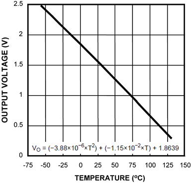
The LMT89 device is a precision analog output CMOS integrated-circuit temperature sensor that operates over a −55°C to 130°C temperature range. The power supply operating range is 2.4 V to 5.5 V. The transfer function of LMT89 device is predominately linear, yet has a slight predictable parabolic curvature. The accuracy of the LMT89 device, when specified to a parabolic transfer function, is typically ±1.5°C at an ambient temperature of 30°C. The temperature error increases linearly and reaches a maximum of ±2.5°C at the temperature range extremes. The temperature range is affected by the power supply voltage. At a power supply voltage of 2.7 V to 5.5 V, the temperature range extremes are 130°C and −55°C. Decreasing the power supply voltage to 2.4 V changes the negative extreme to −30°C, while the positive remains at 130°C.
The quiescent current of the LMT89 device is less than 10 μA. Therefore, self-heating is less than 0.02°C in still air. Shutdown capability for the LMT89 device is intrinsic because its inherent low power consumption allows it to be powered directly from the output of many logic gates or does not necessitate shutdown at all.
The LMT89 device is a cost-competitive alternative to thermistors.
Device Information(1)
| PART NUMBER | PACKAGE | BODY SIZE (NOM) |
|---|---|---|
| LMT89 | SOT (5) | 2.00 mm × 1.25 mm |
- For all available packages, see the orderable addendum at the end of the datasheet.
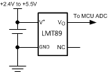
Simplified Schematic
Output Voltage vs Temperature