SNVS056J May 2000 – June 2015 LP3961 , LP3964
PRODUCTION DATA.
- 1 Features
- 2 Applications
- 3 Description
- 4 Revision History
- 5 Pin Configurations and Functions
- 6 Specifications
- 7 Detailed Description
-
8 Application and Implementation
- 8.1 Application Information
- 8.2
Typical Applications
- 8.2.1 Design Requirements
- 8.2.2
Detailed Design Procedure
- 8.2.2.1 External Capacitors
- 8.2.2.2 Selecting a Capacitor
- 8.2.2.3 Capacitor Characteristics
- 8.2.2.4 RFI and EMI Susceptibility
- 8.2.2.5 Output Adjustment
- 8.2.2.6 Turnon Characteristics for Output Voltages Programmed to 2.0 V or Below
- 8.2.2.7 Output Noise
- 8.2.2.8 Shutdown Operation
- 8.2.2.9 Maximum Output Current Capability
- 8.2.3 Application Curves
- 9 Power Supply Recommendations
- 10Layout
- 11Device and Documentation Support
- 12Mechanical, Packaging, and Orderable Information
Package Options
Mechanical Data (Package|Pins)
Thermal pad, mechanical data (Package|Pins)
- KTT|5
Orderable Information
1 Features
- Input Supply Voltage: 2.5 V to 7 V
- Ultra-Low Dropout Voltage
- Low Ground Pin Current
- Load Regulation of 0.02%
- 15-µA Quiescent Current in Shutdown Mode
- Specified Output Current of 0.8-A DC
- Output Voltage Accuracy ±1.5%
- ERROR Flag Indicates Output Status (LP3961)
- Sense Option Improves Better Load Regulation (LP3964)
- Extremely Low Output Capacitor Requirements
- Overtemperature and Overcurrent Protection
- −40°C to 125°C Junction Temperature Range
2 Applications
- Microprocessor Power Supplies
- GTL, GTL+, BTL, and SSTL Bus Terminators
- Power Supplies for DSPs
- SCSI Terminator
- Post Regulators
- High-Efficiency Linear Regulators
- Battery Chargers
- Other Battery-Powered Applications
3 Description
The LP396x series of fast ultra-low-dropout linear regulators operate from a 2.5-V to 7-V input supply. A wide range of preset output voltage options are available. These ultra-low dropout linear regulators respond very fast to step changes in load which makes them suitable for low-voltage microprocessor applications. The LP3961 and LP3964 are developed on a CMOS process which allows low quiescent current operation independent of output load current, as well as operation under extremely low dropout conditions.
Dropout Voltage: Ultra-low dropout voltage; typically 24 mV at 80-mA load current and 240 mV at 800-mA load current.
Ground Pin Current: Typically 4 mA at 800-mA load current.
ERROR Flag:ERROR flag goes low when the output voltage drops 10% below nominal value (for LP3961).
SENSE: SENSE pin improves regulation at remote loads (for LP3964).
Precision Output Voltage: Multiple output voltage options are available ranging from 1.2 V to 5 V and adjustable (LP3964), with a specified accuracy of ±1.5% at room temperature, and ±3% over all conditions (varying line, load, and temperature).
Device Information(1)
| PART NUMBER | PACKAGE | BODY SIZE (NOM) |
|---|---|---|
| LP3961 LP3964 |
SOT-223 (5) | 6.50 mm × 3.56 mm |
| TO-263 (5) | 10.16 mm × 8.42 mm | |
| LP3964 | TO-220 (5) | 14.986 mm × 10.16 mm |
- For all available packages, see the orderable addendum at the end of the data sheet.
space
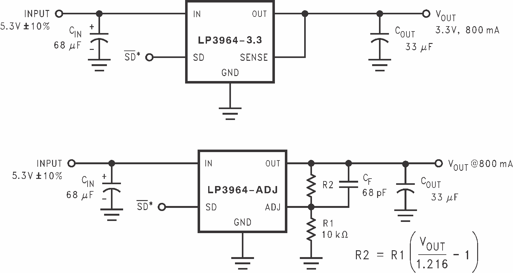
LP3961 Typical Application Circuit

