-
REF19xx Low-Drift, Low-Power, Dual-Output, VREF and VREF / 2 Voltage References
- 1 Features
- 2 Applications
- 3 Description
- 4 Revision History
- 5 Device Comparison Table
- 6 Pin Configuration and Functions
- 7 Specifications
- 8 Parameter Measurement Information
- 9 Detailed Description
- 10Applications and Implementation
- 11Power-Supply Recommendations
- 12Layout
- 13Device and Documentation Support
- 14Mechanical, Packaging, and Orderable Information
- IMPORTANT NOTICE
Package Options
Mechanical Data (Package|Pins)
- DDC|5
Thermal pad, mechanical data (Package|Pins)
Orderable Information
REF19xx Low-Drift, Low-Power, Dual-Output, VREF and VREF / 2 Voltage References
1 Features
- Two Outputs, VREF and VREF / 2, for Convenient Use in Single-Supply Systems
- Excellent Temperature Drift Performance:
- 25 ppm/°C (max) from –40°C to 125°C
- High Initial Accuracy: ±0.1% (max)
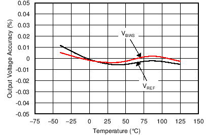
- VREF and VBIAS Tracking over Temperature:
- 6 ppm/°C (max) from –40°C to 85°C
- 7 ppm/°C (max) from –40°C to 125°C
- Microsize Package: SOT23-5
- Low Dropout Voltage: 10 mV
- High Output Current: ±20 mA
- Low Quiescent Current: 360 μA
- Line Regulation: 3 ppm/V
- Load Regulation: 8 ppm/mA
2 Applications
- Digital Signal Processing:
- Power Inverters
- Motor Controls
- Current Sensing
- Industrial Process Controls
- Medical Equipment
- Data Acquisition Systems
- Single-Supply Systems
3 Description
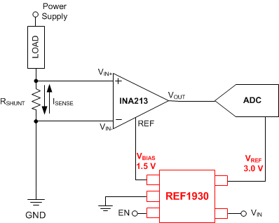
Applications with only a positive supply voltage often require an additional stable voltage in the middle of the analog-to-digital converter (ADC) input range to bias input bipolar signals. The REF19xx provides a reference voltage (VREF) for the ADC and a second highly-accurate voltage (VBIAS) that can be used to bias the input bipolar signals.
The REF19xx offers excellent temperature drift
(25 ppm/°C, max) and initial accuracy (0.1%) on both the VREF and VBIAS outputs while operating at a quiescent current less than 430 µA. In addition, the VREF and VBIAS outputs track each other with a precision of 6 ppm/°C (max) across the temperature range of –40°C to 85°C. All these features increase the precision of the signal chain and decrease board space, while reducing the cost of the system as compared to a discrete solution. Extremely low dropout voltage of only 10 mV allows operation from very low input voltages, which can be very useful in battery-operated systems.
Both the VREF and VBIAS voltages have the same excellent specifications and can sink and source current equally well. Very good long-term stability and low noise levels make these devices ideally-suited for high-precision industrial applications.
Device Information(1)
| PART NAME | PACKAGE | BODY SIZE (NOM) |
|---|---|---|
| REF19xx | SOT (5) | 2.90 mm × 1.60 mm |
- For all available packages, see the orderable addendum at the end of the datasheet.
space
space
Application Example
VREF and VBIAS vs Temperature
4 Revision History
Changes from * Revision (September 2014) to A Revision
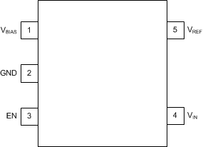
6 Pin Configuration and Functions
7 Specifications
7.1 Absolute Maximum Ratings
over operating free-air temperature range (unless otherwise noted)(1)| MIN | MAX | UNIT | ||
|---|---|---|---|---|
| Input voltage | VIN | –0.3 | 6 | V |
| EN | –0.3 | VIN + 0.3 | ||
| Temperature | Operating | –55 | 150 | °C |
| Junction, TJ | 150 | |||
| Storage, Tstg | –65 | 170 | ||
7.2 ESD Ratings
| VALUE | UNIT | |||
|---|---|---|---|---|
| V(ESD) | Electrostatic discharge | Human-body model (HBM), per ANSI/ESDA/JEDEC JS-001(1) | ±4000 | V |
| Charged-device model (CDM), per JEDEC specification JESD22-C101(2) | ±1500 | |||
7.3 Recommended Operating Conditions
over operating free-air temperature range (unless otherwise noted)| MIN | NOM | MAX | UNIT | ||
|---|---|---|---|---|---|
| VIN | Supply input voltage range (IL = 0 mA, TA = 25°C) | VREF + 0.02(1) | 5.5 | V | |
7.4 Thermal Information
| THERMAL METRIC(1) | REF19xx | UNIT | |
|---|---|---|---|
| DDC (SOT23) | |||
| 5 PINS | |||
| RθJA | Junction-to-ambient thermal resistance | 193.6 | °C/W |
| RθJC(top) | Junction-to-case (top) thermal resistance | 40.2 | °C/W |
| RθJB | Junction-to-board thermal resistance | 34.5 | °C/W |
| ψJT | Junction-to-top characterization parameter | 0.9 | °C/W |
| ψJB | Junction-to-board characterization parameter | 34.3 | °C/W |
| RθJC(bot) | Junction-to-case (bottom) thermal resistance | N/A | °C/W |
7.5 Electrical Characteristics
At TA = 25°C, IL = 0 mA, and VIN = 5 V, unless otherwise noted. Both VREF and VBIAS have the same specifications.| PARAMETER | TEST CONDITIONS | MIN | TYP | MAX | UNIT | |||
|---|---|---|---|---|---|---|---|---|
| ACCURACY AND DRIFT | ||||||||
| Output voltage accuracy | –0.1% | 0.1% | ||||||
| Output voltage temperature coefficient(1) | –40°C ≤ TA ≤ 125°C | ±10 | ±25 | ppm/°C | ||||
| VREF and VBIAS tracking over temperature(2) | –40°C ≤ TA ≤ 85°C | ±1.5 | ±6 | ppm/°C | ||||
| –40°C ≤ TA ≤ 125°C | ±2 | ±7 | ||||||
| LINE AND LOAD REGULATION | ||||||||
| ΔVO(ΔVI) | Line regulation | VREF + 0.02 V ≤ VIN ≤ 5.5 V | 3 | 35 | ppm/V | |||
| ΔVO(ΔIL) | Load regulation | Sourcing | 0 mA ≤ IL ≤ 20 mA , VREF + 0.6 V ≤ VIN ≤ 5.5 V |
8 | 20 | ppm/mA | ||
| Sinking | 0 mA ≤ IL ≤ –20 mA, VREF + 0.02 V ≤ VIN ≤ 5.5 V |
8 | 20 | |||||
| POWER SUPPLY | ||||||||
| ICC | Supply current | Active mode | 360 | 430 | µA | |||
| –40°C ≤ TA ≤ 125°C | 460 | |||||||
| Shutdown mode | 3.3 | 5 | ||||||
| –40°C ≤ TA ≤ 125°C | 9 | |||||||
| Enable voltage | Device in shutdown mode (EN = 0) | 0 | 0.7 | V | ||||
| Device in active mode (EN = 1) | VIN – 0.7 | VIN | ||||||
| Dropout voltage | 10 | 20 | mV | |||||
| IL = 20 mA | 600 | |||||||
| ISC | Short-circuit current | 50 | mA | |||||
| ton | Turn-on time | 0.1% settling, CL = 1 µF | 500 | µs | ||||
| NOISE | ||||||||
| Low-frequency noise(3) | 0.1 Hz ≤ f ≤ 10 Hz | 12 | ppmPP | |||||
| Output voltage noise density | f = 100 Hz | 0.25 | ppm/√Hz | |||||
| CAPACITIVE LOAD | ||||||||
| Stable output capacitor range | 0 | 10 | µF | |||||
| HYSTERESIS AND LONG-TERM STABILITY | ||||||||
| Long-term stability | 0 to 1000 hours | 60 | ppm | |||||
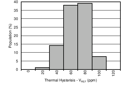
| Output voltage hysteresis(4) | 25°C, –40°C, 125°C, 25°C | Cycle 1 | 60 | ppm | ||||
| Cycle 2 | 35 | |||||||
7.6 Typical Characteristics
At TA = 25°C, IL = 0 mA, VIN = 5-V power supply, CL = 0 µF, and 2.5-V output, unless otherwise noted.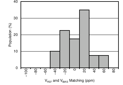
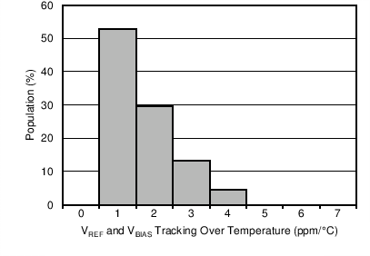
| –40°C ≤ TA ≤ 125°C |
Over Temperature
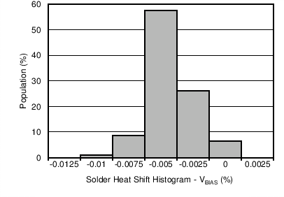
| Refer to the Solder Heat Shift section for more information. |
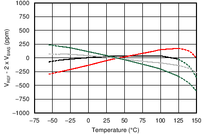
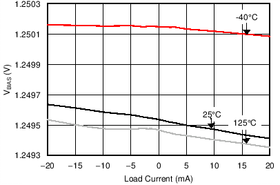
| VBIAS output |
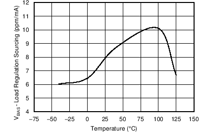
| VBIAS output | IL = 20 mA |
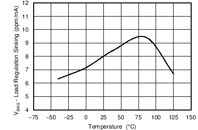
| VBIAS output | IL = –20 mA |
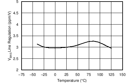
| VBIAS output |
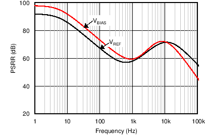
| CL = 10 µF |
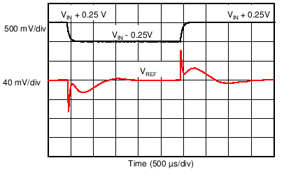
| CL = 10 µF |
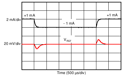
| CL = 10 µF | IL = ±1-mA step |
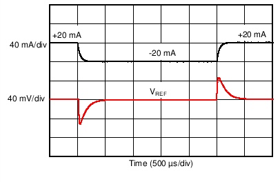
| CL = 10 µF | IL = ±20-mA step |
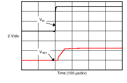
| CL = 1 µF |
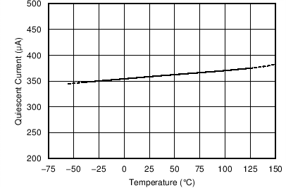
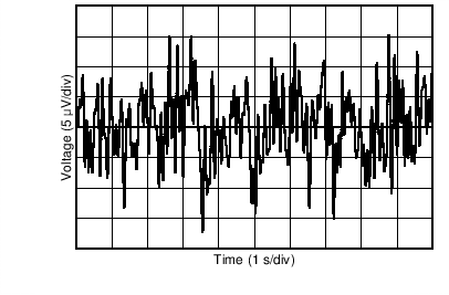
| VREF output |
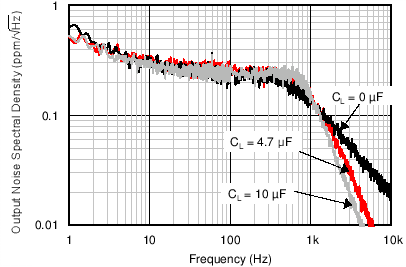
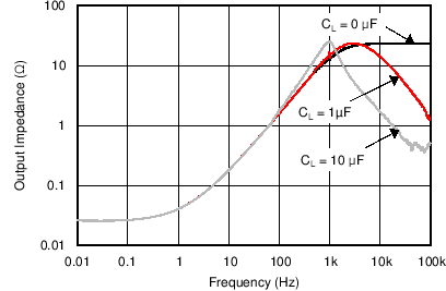
| VBIAS output |
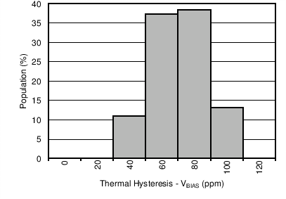
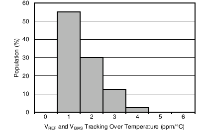
| –40°C ≤ TA ≤ 85°C |
Over Temperature
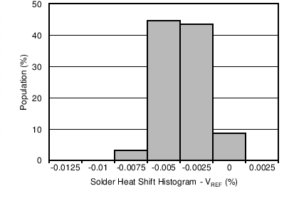
| Refer to the Solder Heat Shift section for more information. |

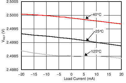
| VREF output |
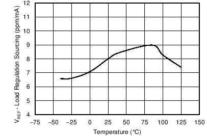
| VREF output | IL = 20 mA |
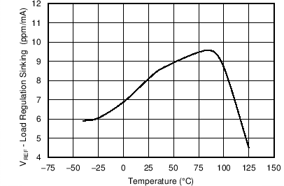
| VREF output | IL = –20 mA |
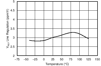
| VREF output |
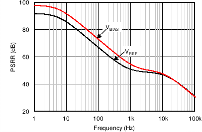
| CL = 0 µF |
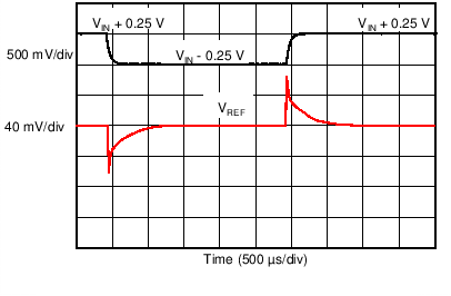
| CL = 1 µF |
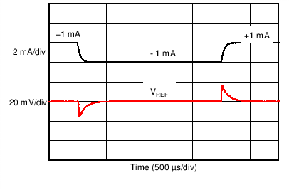
| CL = 1 µF | IL = ±1-mA step |
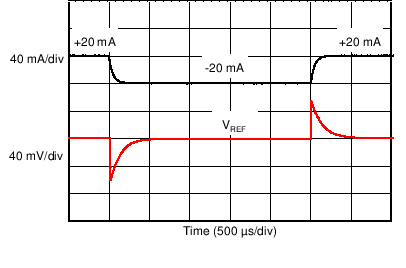
| CL = 1 µF | IL = ±20-mA step |
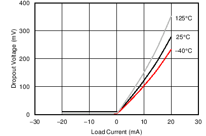
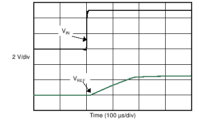
| CL = 10 µF |
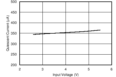
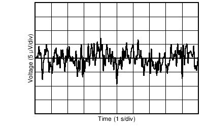
| VBIAS output |
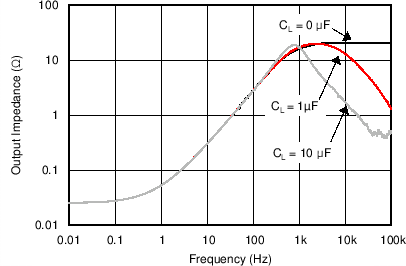
| VREF output |
