SLAS898B January 2014 – April 2015 TAS2552
PRODUCTION DATA.
- 1 Features
- 2 Applications
- 3 Description
- 4 Revision History
- 5 Pin Configuration and Functions
- 6 Specifications
-
7 Detailed Description
- 7.1 Overview
- 7.2 Functional Block Diagram
- 7.3
Feature Description
- 7.3.1 General I2C Operation
- 7.3.2 Single-Byte and Multiple-Byte Transfers
- 7.3.3 Single-Byte Write
- 7.3.4 Multiple-Byte Write and Incremental Multiple-Byte Write
- 7.3.5 Single-Byte Read
- 7.3.6 Multiple-Byte Read
- 7.3.7 PLL
- 7.3.8 Gain Settings
- 7.3.9 Class-D Edge Rate Control
- 7.3.10 Battery Tracking AGC
- 7.3.11 Configurable Boost Current Limit (ILIM)
- 7.4 Device Functional Modes
- 7.5
Register Map
- 7.5.1 Register Map Summary
- 7.5.2 Register 0x00: Device Status Register
- 7.5.3 Register 0x01: Configuration Register 1
- 7.5.4 Register 0x02: Configuration Register 2
- 7.5.5 Register 0x03: Configuration Register 3
- 7.5.6 Register 0x04: DOUT Tristate Mode
- 7.5.7 Register 0x05: Serial Interface Control Register 1
- 7.5.8 Register 0x06: Serial Interface Control Register 2
- 7.5.9 Register 0x07: Output Data Register
- 7.5.10 Register 0x08: PLL Control Register 1
- 7.5.11 Register 0x09: PLL Control Register 2
- 7.5.12 Register 0x0A: PLL Control Register 3
- 7.5.13 Register 0x0B: Battery Tracking Inflection Point Register
- 7.5.14 Register 0x0C: Battery Tracking Slope Control Register
- 7.5.15 Register 0x0D: Reserved Register
- 7.5.16 Register 0x0E: Battery Tracking Limiter Attack Rate and Hysteresis Time
- 7.5.17 Register 0x0F: Battery Tracking Limiter Release Rate
- 7.5.18 Register 0x10: Battery Tracking Limiter Integration Count Control
- 7.5.19 Register 0x11: PDM Configuration Register
- 7.5.20 Register 0x12: PGA Gain Register
- 7.5.21 Register 0x13: Class-D Edge Rate Control Register
- 7.5.22 Register 0x14: Boost Auto-Pass Through Control Register
- 7.5.23 Register 0x15: Reserved Register
- 7.5.24 Register 0x16: Version Number
- 7.5.25 Register 0x17: Reserved Register
- 7.5.26 Register 0x18: Reserved Register
- 7.5.27 Register 0x19: VBAT Data Register
- 8 Applications and Implementation
- 9 Power Supply Recommendations
- 10Layout
- 11Device and Documentation Support
- 12Mechanical, Packaging, and Orderable Information
Package Options
Mechanical Data (Package|Pins)
- YFF|30
Thermal pad, mechanical data (Package|Pins)
Orderable Information
1 Features
- Analog or Digital Input Mono Boosted Class-D Amplifier
- 4.0 W into 8 Ω Load from 4.2 V Supply (1% THD+N)
- Efficiency of 85% at Rated Power
- I2S, Left-Justified, Right-Justified, DSP, PDM, and TDM Input and Output Interface
- Input Sample Rates from 8 kHz to 192 kHz
- High Efficiency Class-G Boost Converter
- Automatically Adjusts Class-D Supply
- Built-In Speaker Sense
- Measures Speaker Current and Voltage
- Measures VBAT and VBOOST Voltages
- Built-In Automatic Gain Control (AGC)
- Limits Battery Current Consumption
- Adjustable Class-D Switching Edge-Rate Control
- Power Supplies
- Boost Input: 3.0 V to 5.5 V
- Analog: 1.65 V to 1.95 V
- Digital I/O: 1.5 V to 3.6 V
- Thermal and Short-Circuit Protection
- I2C Interface for Register Control
- Stereo Configuration Using Two TAS2552s
- I2C Address Select Terminal (ADDR)
- 2.855 mm x 2.575 mm, 0.4 mm Pitch 30-Ball WCSP
2 Applications
- Mobile Phones
- PND
- Portable Audio Docks
- Tablets
- Gaming Devices
3 Description
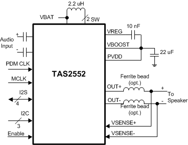
The TAS2552 is a high efficiency Class-D audio power amplifier with advanced battery current management and an integrated Class-G boost converter. The device constantly measures the current and voltage across the load and provides a digital stream of this information.
The Class-G boost converter generates the Class-D amplifier supply rail. During low Class-D output power, the boost improves efficiency by deactivating and connecting VBAT directly to the Class-D amplifier supply. When high power audio is required, the boost quickly activates to provide significantly louder audio than a stand-alone amplifier connected directly to the battery.
The AGC automatically adjusts Class-D gain to reduce battery current at end-of-charge voltages, preventing output clipping, distortion and early system shutdown. The fixed gain is adjustable via I2C. The gain range is -7 dB to +24 dB in 1 dB steps.
In addition to a differential mono analog input, the TAS2552 has built-in a 16-bit D/A converter used with a digital input. Moving the D/A converter from the digital host processor into the integrated amplifier process provides better dynamic performance at lower system cost. Additionally, since the PCB routing is digital rather than analog, sensitivity to external perturbations such as GSM frame-rate noise is decreased at the system level.
Device Information
| ORDER NUMBER | PACKAGE | BODY SIZE |
|---|---|---|
| TAS2552YFF | WCSP (30) | 2.855 mm x 2.575 mm |

4 Revision History
Changes from A Revision (February 2014) to B Revision
- Added clarification on EN Pin Function and ConfigurationGo
- Changed VBAT MAX = 2.45 V. Added footnote to avoid VBAT reset.Go
- Added clarification on wait time regarding DEV_RESET RegisterGo
- Added clarification on VBAT reset range for normal operation mode.Go
Changes from * Revision (January 2014) to A Revision
- Changed from Product Preview to Production Data Go