SLAS988B June 2014 – August 2015 TAS5756M
PRODUCTION DATA.
- 1 Features
- 2 Applications
- 3 Description
- 4 Revision History
- 5 Device Comparison Table
- 6 Pin Configuration and Functions
-
7 Specifications
- 7.1 Absolute Maximum Ratings
- 7.2 ESD Ratings
- 7.3 Recommended Operating Conditions
- 7.4 Thermal Information
- 7.5 Electrical Characteristics
- 7.6 MCLK Timing
- 7.7 Serial Audio Port Timing - Slave Mode
- 7.8 Serial Audio Port Timing - Master Mode
- 7.9 I2C Bus Timing - Standard
- 7.10 I2C Bus Timing - Fast
- 7.11 SPK_MUTE Timing
- 7.12 Power Dissipation
- 7.13 Typical Characteristics
-
8 Detailed Description
- 8.1 Overview
- 8.2 Functional Block Diagram
- 8.3
Feature Description
- 8.3.1 Power-on-Reset (POR) Function
- 8.3.2 Device Clocking
- 8.3.3
Serial Audio Port
- 8.3.3.1 Clock Master Mode from Audio Rate Master Clock
- 8.3.3.2 Clock Master from a Non-Audio Rate Master Clock
- 8.3.3.3 Clock Slave Mode with 4-Wire Operation (SCLK, MCLK, LRCK/FS, SDIN)
- 8.3.3.4 Clock Slave Mode with SLCK PLL to Generate Internal Clocks (3-Wire PCM)
- 8.3.3.5 Serial Audio Port - Data Formats and Bit Depths
- 8.3.3.6 Input Signal Sensing (Power-Save Mode)
- 8.3.3.7 Serial Data Output
- 8.3.4 Modulation Scheme
- 8.3.5 miniDSP Audio Processing Engine
- 8.3.6 Adjustable Amplifier Gain and Switching Frequency Selection
- 8.3.7
Error Handling and Protection Suite
- 8.3.7.1 Device Overtemperature Protection
- 8.3.7.2 SPK_OUTxx Overcurrent Protection
- 8.3.7.3 DC Offset Protection
- 8.3.7.4 Internal VAVDD Undervoltage-Error Protection
- 8.3.7.5 Internal VPVDD Undervoltage-Error Protection
- 8.3.7.6 Internal VPVDD Overvoltage-Error Protection
- 8.3.7.7 External Undervoltage-Error Protection
- 8.3.7.8 Internal Clock Error Notification (CLKE)
- 8.3.8 GPIO Port and Hardware Control Pins
- 8.3.9 I2C Communication Port
- 8.4 Device Functional Modes
-
9 Application and Implementation
- 9.1 Application Information
- 9.2
Typical Applications
- 9.2.1 2.0 (Stereo BTL) System
- 9.2.2 Mono (PBTL) Systems
- 9.2.3 2.1 (Stereo BTL + External Mono Amplifier) Systems
- 9.2.4 2.2 (Dual Stereo BTL) Systems
- 9.2.5 1.1 (Dual BTL, Bi-Amped) Systems
- 10Power Supply Recommendations
- 11Layout
- 12Device and Documentation Support
- 13Mechanical, Packaging, and Orderable Information
Package Options
Mechanical Data (Package|Pins)
- DCA|48
Thermal pad, mechanical data (Package|Pins)
- DCA|48
Orderable Information
1 Features
- Flexible Audio I/O Configuration
- Supports I2S, TDM, LJ, RJ Digital Input
- 8 kHz to 192 kHz Sample Rate Support
- Stereo Bridge Tied Load (BTL) or Mono Parallel Bridge Tied Load (PBTL) Operation
- BD Amplifier Modulation
- Supports 3-Wire Digital Audio Interface (No MCLK required)
- High-Performance Closed-Loop Architecture (PVDD = 12V, RSPK = 8 Ω, SPK_GAIN = 20 dBV)
- Idle Channel Noise = 56 µVrms (A-Wtd)
- THD+N = 0.006 % (at 1 W, 1 kHz)
- SNR = 104 A-Wtd (Ref. to THD+N = 1%)
-
PurePath™ HybridFlow Processing Architecture
- Several Configurable MiniDSP Programs (called HybridFlows)
- Download Time <100 ms (typ)
- Advanced Audio Processing Algorithms (2)
- Communication Features
- Software Mode Control via I2C Port
- Two Address Select Pins – Up to 4 Devices
- Robustness and Reliability Features
- Clock Error, DC, and Short-Circuit Protection
- Over Temperature and Overcurrent Protection
2 Applications
- LCD, LED TV, and Multi-Purpose Monitors
- Sound Bars, Docking Stations, PC Audio
- Wireless Subwoofers, Bluetooth and Active Speakers
3 Description
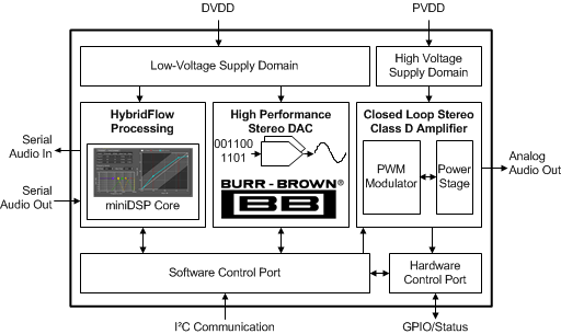
The TAS5756M device is a high-performance, stereo closed-loop amplifier with integrated audio processor with architecture. To convert from digital to analog, the device uses a high performance DAC with Burr-Brown® mixed signal heritage. It requires only two power supplies; one DVDD for low-voltage circuitry and one PVDD for high-voltage circuitry. It is controlled by a software control port using standard I2C communication. In the family, the TAS5756M uses traditional BD modulation, ensuring low distortion characteristics. The TAS5754M uses 1SPW modulation to reduce output ripple current, the expense of slightly higher distortion.
The unique HybridFlow architecture allows the system designer to choose from several configurable DSP programs that are specifically designed for use in popular audio end equipment such as bluetooth (BT) speakers, sound bars, docking stations, and subwoofers. This architecture combines the flexibility of a fully programmable device with the fast download time and ease of use of a fixed-function ROM device.
An optimal mix of thermal performance and device cost is provided in the 90 mΩ rDS(on) of the output MOSFETs. Additionally, a thermally enhanced 48-Pin HTSSOP provides excellent operation in the elevated ambient temperatures found in modern consumer electronic devices.
Device Information(1)
| PART NUMBER | PACKAGE | BODY SIZE (NOM) |
|---|---|---|
| TAS5756M | HTSSOP (48) | 12.50 mm × 6.10 mm |
- For all available packages, see the orderable addendum at the end of the datasheet.
- Please refer to SLAU577 for information regarding Audio Processing options available via the HybridFlow library.
- Tested on TAS5756MDCAEVM.
Simplified Block Diagram

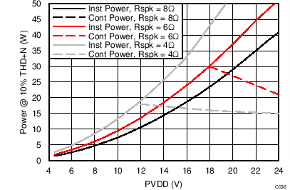
Power at 10% THD+N vs PVDD(3)
