SLVS029H January 1984 – November 2015 TL499A
PRODUCTION DATA.
- 1 Features
- 2 Applications
- 3 Description
- 4 Revision History
- 5 Pin Configuration and Functions
- 6 Specifications
- 7 Detailed Description
- 8 Application and Implementation
- 9 Power Supply Recommendations
- 10Layout
- 11Device and Documentation Support
- 12Mechanical, Packaging, and Orderable Information
Package Options
Refer to the PDF data sheet for device specific package drawings
Mechanical Data (Package|Pins)
- P|8
- PS|8
Thermal pad, mechanical data (Package|Pins)
Orderable Information
1 Features
2 Applications
- Voltage Boosting
- Dual-Supply Voltage Reglation
- Battery Back-Ups
- Microprocessor Memory Power
3 Description
The TL499A device is an integrated circuit designed to provide a wide range of adjustable regulated supply voltages. The regulated output voltage can be varied from 2.9 V to 30 V by adjusting two external resistors. When the TL499A is ac-coupled to line power through a step-down transformer, it operates as a series DC voltage regulator to maintain the regulated output voltage. With the addition of a battery from 1.1 V to 10 V, an inductor, a filter capacitor, and two resistors, the TL499A operates as a step-up switching regulator during an AC-line failure. The adjustable regulated output voltage makes the TL499A useful for a wide range of applications. Providing backup power during an AC-line failure makes the TL499A extremely useful in microprocessor memory applications. The TL499AC is characterized for operation from –20°C to +85°C.
Device Information(1)
| PART NUMBER | PACKAGE (PIN) | BODY SIZE (NOM) |
|---|---|---|
| TL499A | SO (8) | 6.20 mm × 5.30 mm |
| PDIP (8) | 9.81 mm × 6.35 mm |
- For all available packages, see the orderable addendum at the end of the data sheet.
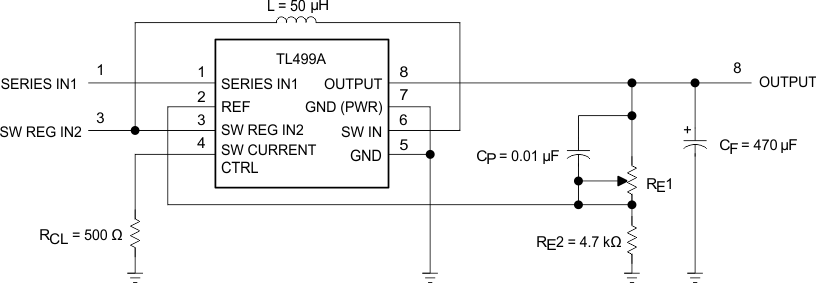
Typical Application
