TLV431x Low-Voltage Adjustable Precision Shunt Regulator
1 Features
- Low-voltage operation, VREF = 1.24V
- Adjustable output voltage, VO = VREF to 6V
- Reference voltage tolerances at
25°C
- 0.5% for TLV431B
- 1% for TLV431A
- 1.5% for TLV431
- Typical temperature drift
- 4mV (0°C to 70°C)
- 6mV (–40°C to 85°C)
- 11mV (–40°C to 125°C)
- Low operational cathode current, 80µA typical
- 0.25Ω typical output impedance
- Ultra-small SC-70 package offers 40% smaller footprint than SOT-23-3
- See TLVH431 and TLVH432 for:
- Wider VKA (1.24V to 18 V) and IK (80mA)
- Additional SOT-89 package
- Multiple pinouts for SOT-23-3 and SOT-89 packages
- On products compliant to MIL-PRF-38535, all parameters are tested unless otherwise noted. on all other products, production processing does not necessarily include testing of all parameters.
2 Applications

3 Description
The TLV431 device is a low-voltage 3-terminal adjustable voltage reference with specified thermal stability over applicable industrial and commercial temperature ranges. Output voltage can be set to any value between VREF (1.24V) and 6V with two external resistors (see the Parameter Measurement Information section). These devices operate from a lower voltage (1.24V) than the widely used TL431 and TL1431 shunt-regulator references.
When used with an optocoupler, the TLV431 device is an ideal voltage reference in isolated feedback circuits for 3V to 3.3V switching-mode power supplies. These devices have a typical output impedance of 0.25Ω. Active output circuitry provides a very sharp turnon characteristic, making them excellent replacements for low-voltage Zener diodes in many applications, including on-board regulation and adjustable power supplies.
| PART NUMBER | PACKAGE(1) | PACKAGE SIZE(2) |
|---|---|---|
| TLV431 | DBZ (SOT-23, 3) | 2.92mm × 2.37mm |
| DBV (SOT-23, 5) | 2.90mm × 2.8mm | |
| LP (TO-92, 3) | 5.2mm × 3.68mm | |
| PK (SOT-89, 3) | 4.5mm × 4.095mm | |
| TLV431A | DBV (SOT-23, 5) | 2.90mm × 2.8mm |
| DBZ (SOT-23, 3) | 2.92mm × 2.37mm | |
| PK (SOT-89, 3) | 4.5mm × 4.095mm | |
| LP (TO-92, 3) | 5.2mm × 3.68mm | |
| D (SOIC, 8) | 4.9mm × 6mm | |
| TLV431B | DBV (SOT-23, 5) | 2.90mm × 2.8mm |
| DBZ (SOT-23, 3) | 2.92mm × 2.37mm | |
| PK (SOT-89, 3) | 4.5mm × 4.095mm | |
| LP (TO-92, 3) | 5.2mm × 3.68mm | |
| DCK (SOT-SC70, 6) | 2mm × 1.5mm |
4 Pin Configuration and Functions
 Package (Top View)") Figure 4-1 D (SOIC) Package
Figure 4-1 D (SOIC) Package (Top View)
 Package (Top View)") Figure 4-3 DBZ (SOT-23-3) Package
Figure 4-3 DBZ (SOT-23-3) Package(Top View)
 Package (Top View)") Figure 4-5 DCK (SC-70) Package
Figure 4-5 DCK (SC-70) Package(Top View)
 Package (Top View)")
NC − No internal connection
* Pin 2 is attached to Substrate and must be connected to ANODE or left open.
Figure 4-2 DBV (SOT-23-5) Package(Top View)
 Package (Top View)") Figure 4-4 PK (SOT-89) Package
Figure 4-4 PK (SOT-89) Package (Top View)
 Package
(Top View)") Figure 4-6 LP (TO-92/TO-226) Package
Figure 4-6 LP (TO-92/TO-226) Package
(Top View)
| PIN | TYPE | DESCRIPTION | ||||||
|---|---|---|---|---|---|---|---|---|
| NAME | DBZ | DBV | PK | D | LP | DCK | ||
| CATHODE | 2 | 3 | 3 | 1 | 1 | 1 | I/O | Shunt Current/Voltage input |
| REF | 1 | 4 | 1 | 8 | 3 | 3 | I | Threshold relative to common anode |
| ANODE | 3 | 5 | 2 | 2, 3, 6, 7 | 2 | 6 | O | Common pin, normally connected to ground |
| NC | — | 1 | — | 4, 5 | — | 4, 5 | I | No Internal Connection |
| * | — | 2 | — | — | — | 2 | I | Substrate Connection. Must be connected to ANODE or left open. |
5 Specifications
5.1 Absolute Maximum Ratings
| MIN | MAX | UNIT | ||
|---|---|---|---|---|
| VKA | Cathode voltage (2) | 7 | V | |
| IK | Continuous cathode current | –20 | 20 | mA |
| Iref | Reference current | –0.05 | 3 | mA |
| Operating virtual junction temperature | 150 | °C | ||
| Tstg | Storage temperature | –65 | 150 | °C |
5.2 ESD Ratings
| PARAMETER | DEFINITION | VALUE | UNIT | |
|---|---|---|---|---|
| V(ESD) | Electrostatic discharge | Human body model (HBM), per ANSI/ESDA/JEDEC JS-001, all pins (1) | ±2000 | V |
| Charged device model (CDM), per JEDEC specification JESD22-C101, all pins (2) | ±1000 | |||
5.3 Recommended Operating Conditions
| MIN | MAX | UNIT | |||
|---|---|---|---|---|---|
| VKA | Cathode voltage | VREF | 6 | V | |
| IK | Cathode current | 0.1 | 15 | mA | |
| TA | Operating free-air temperature | TLV431_C | 0 | 70 | °C |
| TLV431_I | –40 | 85 | |||
| TLV431_Q | –40 | 125 | |||
5.4 Thermal Information
| THERMAL METRIC (1) | TLV431x | UNIT | ||||||
|---|---|---|---|---|---|---|---|---|
| DCK | D | PK | DBV | DBZ | LP | |||
| 6 PINS | 8 PINS | 3 PINS | 5 PINS | 3 PINS | 3 PINS | |||
| RθJA | Junction-to-ambient thermal resistance | 87 | 97 | 52 | 206 | 206 | 140 | °C/W |
| RθJC(top) | Junction-to-case (top) thermal resistance | 259 | 39 | 9 | 131 | 76 | 55 | °C/W |
5.5 Electrical Characteristics for TLV431
| PARAMETER | TEST CONDITIONS | TLV431 | UNIT | |||||
|---|---|---|---|---|---|---|---|---|
| MIN | TYP | MAX | ||||||
| VREF | Reference voltage | VKA = VREF, IK=10mA | TA = 25°C | 1.222 | 1.24 | 1.258 | V | |
| TA = full range (1) (see Figure 6-1) | TLV431C | 1.21 | 1.27 | |||||
| TLV431I | 1.202 | 1.278 | ||||||
| TLV431Q | 1.194 | 1.286 | ||||||
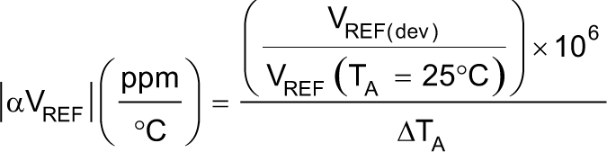
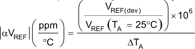
| VREF(dev) | VREF deviation over full temperature range(2) | VKA = VREF, IK = 10mA (1) (see Figure 6-1) | TLV431C | 4 | 12 | mV | ||
| TLV431I | 6 | 20 | ||||||
| TLV431Q | 11 | 31 | ||||||

|
Ratio of VREF change in cathode voltage change | VKA = VREF to 6V, IK = 10mA (see Figure 6-2) | -1.5 | -2.7 | mV/V | |||
| Iref | Reference terminal current | IK = 10mA, R1 = 10kΩ, R2 = open (see Figure 6-2) | 0.15 | 0.5 | µA | |||
| Iref(dev) | Iref deviation over full temperature range(2) | IK = 10mA, R1 =10kΩ, R2 = open (1) (see Figure 6-2) | TLV431C | 0.05 | 0.3 | µA | ||
| TLV431I | 0.1 | 0.4 | ||||||
| TLV431Q | 0.15 | 0.5 | ||||||
| IK(min) | Minimum cathode current for regulation | VKA = VREF (see Figure 6-1) | TLV431C/I | 55 | 80 | µA | ||
| TLV431Q | 55 | 100 | ||||||
| IK(off) | Off-state cathode current | VREF = 0, VKA = 6V (see Figure 6-3) | 0.001 | 0.1 | µA | |||
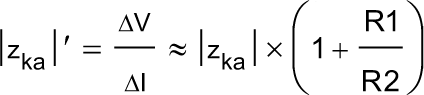
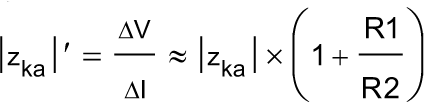
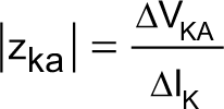
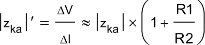
| |zKA| | Dynamic impedance(3) | VKA = VREF, f ≤ 1kHz, IK = 0.1mA to 15mA (see Figure 6-1) | 0.25 | 0.4 | Ω | |||
 . When the
device is operating with two external resistors (see Figure 6-2), the total dynamic impedance of the circuit is defined as:
. When the
device is operating with two external resistors (see Figure 6-2), the total dynamic impedance of the circuit is defined as:
5.6 Electrical Characteristics for TLV431A
| PARAMETER | TEST CONDITIONS | TLV431A | UNIT | |||||
|---|---|---|---|---|---|---|---|---|
| MIN | TYP | MAX | ||||||
| VREF | Reference voltage | VKA = VREF, IK = 10mA | TA = 25°C | 1.228 | 1.24 | 1.252 | V | |
| TA = full range (1) (see Figure 6-1) | TLV431AC | 1.221 | 1.259 | |||||
| TLV431AI | 1.215 | 1.265 | ||||||
| TLV431AQ | 1.209 | 1.271 | ||||||
| VREF(dev) | VREF deviation over full temperature range (2) | VKA = VREF, IK = 10mA (1) (see Figure 6-1) | TLV431AC | 4 | 12 | mV | ||
| TLV431AI | 6 | 20 | ||||||
| TLV431AQ | 11 | 31 | ||||||
|
Ratio of VREF change in cathode voltage change | VKA = VREF to 6V, IK = 10mA (see Figure 6-2) | -1.5 | -2.7 | mV/V | |||
| Iref | Reference terminal current | IK = 10mA, R1 = 10kΩ, R2 = open (see Figure 6-2) | 0.15 | 0.5 | µA | |||
| Iref(dev) | Iref deviation over full temperature range (2) | IK = 10mA, R1 = 10kΩ, R2 = open(1) (see Figure 6-2) | TLV431AC | 0.05 | 0.3 | µA | ||
| TLV431AI | 0.1 | 0.4 | ||||||
| TLV431AQ | 0.15 | 0.5 | ||||||
| IK(min) | Minimum cathode current for regulation | VKA = VREF (see Figure 6-1) | TLV431AC/AI | 55 | 80 | µA | ||
| TLV431AQ | 55 | 100 | ||||||
| IK(off) | Off-state cathode current | VREF = 0, VKA = 6V (see Figure 6-3) | 0.001 | 0.1 | µA | |||
| |zKA| | Dynamic impedance (3) | VKA = VREF, f ≤ 1kHz, IK = 0.1mA to 15mA (see Figure 6-1) | 0.25 | 0.4 | Ω | |||
 . When
the device is operating with two external resistors (see Figure 6-2), the total dynamic impedance of the circuit is defined as:
. When
the device is operating with two external resistors (see Figure 6-2), the total dynamic impedance of the circuit is defined as:
5.7 Electrical Characteristics for TLV431B
| PARAMETER | TEST CONDITIONS | TLV431B | UNIT | |||||
|---|---|---|---|---|---|---|---|---|
| MIN | TYP | MAX | ||||||
| VREF | Reference voltage | VKA = VREF, IK=10mA | TA = 25°C | 1.234 | 1.24 | 1.246 | V | |
| TA = full range (1) (see Figure 6-1) | TLV431BC | 1.227 | 1.253 | |||||
| TLV431BI | 1.224 | 1.259 | ||||||
| TLV431BQ | 1.221 | 1.265 | ||||||
| VREF(dev) | VREF deviation over full temperature range (2) | VKA = VREF , IK = 10mA (1) (see Figure 6-1) | TLV431BC | 4 | 12 | mV | ||
| TLV431BI | 6 | 20 | ||||||
| TLV431BQ | 11 | 31 | ||||||

|
Ratio of VREF change in cathode voltage change | VKA = VREF to 6V, IK = 10mA (see Figure 6-2) | -1.5 | -2.7 | mV/V | |||
| Iref | Reference terminal current | IK = 10mA, R1 = 10kΩ, R2 = open (see Figure 6-2) | 0.1 | 0.5 | µA | |||
| Iref(dev) | Iref deviation over full temperature range (2) | IK = 10mA, R1 =10kΩ, R2 = open (3) (see Figure 6-2) | TLV431BC | 0.05 | 0.3 | µA | ||
| TLV431BI | 0.1 | 0.4 | ||||||
| TLV431BQ | 0.15 | 0.5 | ||||||
| IK(min) | Minimum cathode current for regulation | VKA = VREF (see Figure 6-1) | 55 | 100 | µA | |||
| IK(off) | Off-state cathode current | VREF = 0, VKA = 6V (see Figure 6-3) | 0.001 | 0.1 | µA | |||
| |zKA| | Dynamic impedance (4) | VKA = VREF, f ≤ 1kHz, IK = 0.1mA to 15mA (see Figure 6-1) | 0.25 | 0.4 | Ω | |||

 . When
the device is operating with two external resistors (see Figure 6-2), the total dynamic impedance of the circuit is defined as:
. When
the device is operating with two external resistors (see Figure 6-2), the total dynamic impedance of the circuit is defined as:
5.8 Typical Characteristics
Operation of the device at these or any other conditions beyond those indicated in the Recommended Operating Conditions table are not implied.
 Figure 5-1 Reference Voltage vs Junction Temperature
") Figure 5-3 Reference Input Current vs Junction Temperature (for TLV431B)
Figure 5-3 Reference Input Current vs Junction Temperature (for TLV431B) Figure 5-5 Minimum Cathode Current vs Temperature
") Figure 5-7 Off-State Cathode Current vs Junction Temperature (for TLV431 and
TLV431A)
Figure 5-7 Off-State Cathode Current vs Junction Temperature (for TLV431 and
TLV431A)") Figure 5-9 Ratio of Delta Reference Voltage to Delta Cathode Voltage vs Junction
Temperature (for TLV431 and TLV431A)
Figure 5-9 Ratio of Delta Reference Voltage to Delta Cathode Voltage vs Junction
Temperature (for TLV431 and TLV431A)‡Extrapolated from Life-test Data Taken at 125°C; the Activation Energy Assumed Is 0.7 eV.
 Figure 5-11 Percentage Change in vREF vs Operating Life at 55°C
") Figure 5-2 Reference Input Current vs Junction Temperature (for TLV431 and
TLV431A)
Figure 5-2 Reference Input Current vs Junction Temperature (for TLV431 and
TLV431A) Figure 5-4 Cathode Current vs Cathode Voltage
 Figure 5-6 Cathode Current vs Cathode Voltage
") Figure 5-8 Off-State Cathode Current vs Junction Temperature (for TLV431B)
Figure 5-8 Off-State Cathode Current vs Junction Temperature (for TLV431B)") Figure 5-10 Ratio of Delta Reference Voltage to Delta Cathode Voltage vs Junction
Temperature (for TLV431B)
Figure 5-10 Ratio of Delta Reference Voltage to Delta Cathode Voltage vs Junction
Temperature (for TLV431B) Figure 5-12 Equivalent Input Noise
Voltage
Figure 5-12 Equivalent Input Noise
Voltage Figure 5-13 Equivalent Noise Voltage
over a 10S Period
Figure 5-13 Equivalent Noise Voltage
over a 10S Period Figure 5-14 Voltage Gain and Phase
Margin
Figure 5-14 Voltage Gain and Phase
Margin Figure 5-15 Reference Impedance vs
Frequency
Figure 5-15 Reference Impedance vs
Frequency Figure 5-16 Pulse Response 1
 Figure 5-17 Pulse Response 2
, TA= 25°C") Figure 5-19 Phase Margin vs Capacitive
Load vKA = VREF (1.25V), TA= 25°C
Figure 5-19 Phase Margin vs Capacitive
Load vKA = VREF (1.25V), TA= 25°C Figure 5-20 Phase Margin vs Capacitive
Load vKA = 2.50V, TA= 25°C
Figure 5-20 Phase Margin vs Capacitive
Load vKA = 2.50V, TA= 25°C Figure 5-21 Phase Margin vs Capacitive
Load vKA = 5.00V, TA= 25°C
Figure 5-21 Phase Margin vs Capacitive
Load vKA = 5.00V, TA= 25°C6 Parameter Measurement Information
 Figure 6-1 Test Circuit for vKA = VREF, VO = VKA = VREF
 + Iref × R1") Figure 6-2 Test Circuit for vKA > VREF, VO = VKA = VREF × (1 + R1/R2) + Iref × R1
Figure 6-2 Test Circuit for vKA > VREF, VO = VKA = VREF × (1 + R1/R2) + Iref × R1") Figure 6-3 Test Circuit for IK(off)
Figure 6-3 Test Circuit for IK(off)
7 Detailed Description
7.1 Overview
TLV431 is a low power counterpart to TL431, having lower reference voltage (1.24V vs 2.5 V) for lower voltage adjustability and lower minimum cathode current (Ik(min)= 100µA vs 1mA). Like TL431, TLV431 is used in conjunction with it's key components to behave as a single voltage reference, error amplifier, voltage clamp, or comparator with integrated reference.
TLV431 can be operated and adjusted to cathode voltages from 1.24V to 6V, making this part optimum for a wide range of end equipments in industrial, auto, telecom, and computing. For this device to behave as a shunt regulator or error amplifier, > 100µA (Imin(max)) must be supplied in to the cathode pin. Under this condition, feedback can be applied from the Cathode and Ref pins to create a replica of the internal reference voltage.
Various reference voltage options can be purchased with initial tolerances (at 25°C) of 0.5%, 1%, and 1.5%. These reference options are denoted by B (0.5%), A (1.0%), and blank (1.5%) after the TLV431.
The TLV431xC devices are characterized for operation from 0°C to 70°C, the TLV431xI devices are characterized for operation from –40°C to 85°C, and the TLV431xQ devices are characterized for operation from –40°C to 125°C.
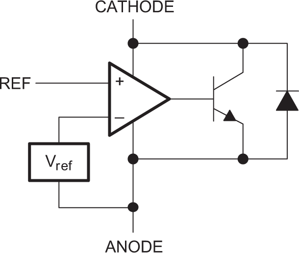
7.2 Functional Block Diagram
7.3 Feature Description
TLV431 consists of an internal reference and amplifier that outputs a sink current base on the difference between the reference pin and the virtual internal pin. The sink current is produced by an internal darlington pair.
When operated with enough voltage headroom (≥ 1.24V) and cathode current (Ika), TLV431 forces the reference pin to 1.24V. However, the reference pin can not be left floating, as it requires Iref ≥ 0.5µA (see the Functional Block Diagram). This is because the reference pin is driven into an NPN, which requires a base current to operate properly.
When feedback is applied from the Cathode and Reference pins, TLV431 behaves as a Zener diode, regulating to a constant voltage dependent on current being supplied into the cathode. This is due to the internal amplifier and reference entering the proper operating regions. The same amount of current required in the above feedback situation must be applied to this device in open-loop, servo, or error-amplifying implementations for it to be in the proper linear region giving TLV431 enough gain.
Unlike many linear regulators, TLV431 is internally compensated to be stable without an output capacitor between the cathode and anode. However, if it is desired to use an output capacitor Figure 5-19 can be used as a guide to assist in choosing the correct capacitor to maintain stability.