SLOS474E August 2005 – March 2016 TPA2005D1-Q1
PRODUCTION DATA.
- 1 Features
- 2 Applications
- 3 Description
- 4 Revision History
- 5 Device Comparison Table
- 6 Pin Configuration and Functions
- 7 Specifications
- 8 Parameter Measurement Information
- 9 Detailed Description
- 10Application and Implementation
- 11Power Supply Recommendations
- 12Layout
- 13Device and Documentation Support
- 14Mechanical, Packaging, and Orderable Information
Package Options
Mechanical Data (Package|Pins)
Thermal pad, mechanical data (Package|Pins)
Orderable Information
1 Features
- Qualified for Automotive Applications
- AEC-Q100 Qualified With the Following Results:
- Device Temperature Grade 3 (DRB and DGN package non T-suffix): –40°C to +85°C Ambient Operating Temperature Range
- Device Temperature Grade 2 (DGN package T-suffix): –40°C to +105°C Ambient Operating Temperature Range
- Device HBM Classification Level 2
- Device CDM Classification Level C5
- 1.4 W Into 8 Ω From a 5-V Supply at
THD = 10% (Typical) - Maximum Battery Life and Minimum Heat
- Efficiency With an 8-Ω Speaker:
- 84% at 400 mW
- 79% at 100 mW
- 2.8-mA Quiescent Current
- 0.5-μA Shutdown Current
- Efficiency With an 8-Ω Speaker:
- Only Three External Components
- Optimized PWM Output Stage Eliminates LC Output Filter
- Internally Generated 250-kHz Switching Frequency Eliminates Capacitor and Resistor
- Improved PSRR (–71 dB at 217 Hz) and Wide Supply Voltage (2.5 V to 5.5 V) Eliminates Need for a Voltage Regulator
- Fully Differential Design Reduces RF Rectification and Eliminates Bypass Capacitor
- Improved CMRR Eliminates Two Input Coupling Capacitors
- Space-Saving Packages
2 Applications
- Cluster
- Head Unit
- Telematics
- Emergency Call (eCall)
- Noise Generator
3 Description
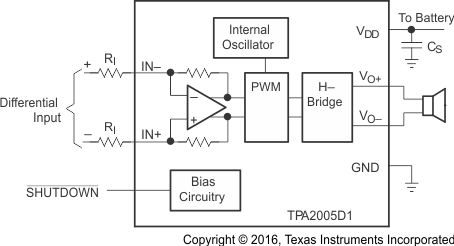
The TPA2005D1-Q1 device is a 1.4-W high-efficiency filter-free class-D audio power amplifier in a SON or MSOP-PowerPAD package that requires only three external components.
Features like 84% efficiency, –71-dB PSRR at 217 Hz, improved RF-rectification immunity, and 15-mm2 total PCB area make TPA2005D1-Q1 ideal for low-power audio applications in infotainment and cluster.
The device allows for independent gain control by summing the signals from each function while minimizing noise to only 48 µVRMS. Additionally, the TPA2005D1-Q1 device offers fast start-up time of 9 ms with minimal pop and has short circuit and thermal protection.
Device Information(1)
| PART NUMBER | PACKAGE | BODY SIZE (NOM) |
|---|---|---|
| TPA2005D1-Q1 | MSOP-PowerPAD (8) | 3.00 mm × 3.00 mm |
| SON (8) | 3.00 mm × 3.00 mm |
- For all available packages, see the orderable addendum at the end of the data sheet.
