SLVSAU6H June 2011 – April 2016 TPS2000C , TPS2001C , TPS2041C , TPS2051C , TPS2061C , TPS2065C , TPS2065C-2 , TPS2068C , TPS2069C , TPS2069C-2
PRODUCTION DATA.
- 1 Features
- 2 Applications
- 3 Description
- 4 Revision History
- 5 Device Comparison Table
- 6 Pin Configuration and Functions
-
7 Specifications
- 7.1 Absolute Maximum Ratings
- 7.2 ESD Ratings
- 7.3 Recommended Operating Conditions
- 7.4 Thermal Information: SOT-23
- 7.5 Thermal Information: MSOP-PowerPAD
- 7.6 Electrical Characteristics: TJ = TA = 25°C
- 7.7 Electrical Characteristics: -40°C ≤ TJ ≤ 125°C
- 7.8 Timing Requirements: TJ = TA = 25°C
- 7.9 Typical Characteristics
- 8 Detailed Description
- 9 Application and Implementation
- 10Power Supply Recommendations
- 11Layout
- 12Device and Documentation Support
- 13Mechanical, Packaging, and Orderable Information
Package Options
Mechanical Data (Package|Pins)
Thermal pad, mechanical data (Package|Pins)
- DGN|8
Orderable Information
1 Features
- Single Power Switch Family
- Pin-for-Pin With Existing TI Switch Portfolio
- Rated Currents of 0.5 A, 1 A, 1.5 A, 2 A
- ±20% Accurate, Fixed, Constant Current Limit
- Fast Overcurrent Response: 2 µs
- Deglitched Fault Reporting
- Selected Parts With (TPS20xxC) and Without (TPS20xxC-2) Output Discharge
- Reverse Current Blocking
- Built-In Soft Start
- Ambient Temperature Range: –40°C to 85°C
- UL Listed and CB-File No. E169910
2 Applications
- USB Ports and Hubs, Laptops, and Desktops
- High-Definition Digital TVs
- Set-Top Boxes
- Short-Circuit Protection
3 Description
The TPS20xxC and TPS20xxC-2 power-distribution switch family is intended for applications, such as USB, where heavy capacitive loads and short circuits are likely to be encountered. This family offers multiple devices with fixed current-limit thresholds for applications from 0.5 A to 2 A.
The TPS20xxC and TPS20xxC-2 family limits the output current to a safe level by operating in a constant-current mode when the output load exceeds the current limit threshold. This provides a predictable fault current under all conditions. The fast overload response time eases the burden on the main 5-V supply to provide regulated power when the output is shorted. The power-switch rise and fall times are controlled to minimize current surges during turnon and turnoff.
Device Information(1)
| PART NUMBER | PACKAGE | BODY SIZE (NOM) |
|---|---|---|
| TPS20xxC, TPS20xxC-2 |
SOT-23 (5) | 2.90 mm × 1.60 mm |
| VSSOP (8) | 3.00 mm × 3.00 mm | |
| MSOP-PowerPAD (8) | 3.00 mm × 3.00 mm |
- For all available packages, see the orderable addendum at the end of the data sheet.
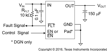
Typical Application Diagram
