-
TPS2115A-Q1 Auto-Switching Power Multiplexer
- 1 Features
- 2 Applications
- 3 Description
- 4 Revision History
- 5 Pin Configuration and Functions
- 6 Specifications
- 7 Parameter Measurement Information
- 8 Detailed Description
- 9 Application and Information
- 10Power Supply Recommendations
- 11Layout
- 12Device and Documentation Support
- 13Mechanical, Packaging, and Orderable Information
- IMPORTANT NOTICE
Package Options
Mechanical Data (Package|Pins)
- PW|8
Thermal pad, mechanical data (Package|Pins)
Orderable Information
DATA SHEET
TPS2115A-Q1 Auto-Switching Power Multiplexer
1 Features
- Qualified for Automotive Applications
- AEC-Q100 Qualified With the Following Results:
- Device Temperature Grade 3: –40°C to 85°C Ambient Operating Temperature Range
- Device HBM ESD Classification Level 2
- Device CDM ESD Classification Level C4A
- Two-Input One-Output Power Multiplexer With Low rDS(on) Switch...84 mΩ (Typical)
- Reverse and Cross-Conduction Blocking
- Wide Operating Voltage Range...2.8 V to 5.5 V
- Low Standby Current...0.5 μA (Typical)
- Low Operating Current...55 μA (Typical)
- Adjustable Current Limit
- Controlled Output-Voltage Transition Times Limit Inrush Current and Minimize Output Voltage Hold-Up Capacitance
- CMOS- and TTL-Compatible Control Inputs
- Manual and Auto-Switching Operating Modes
- Thermal Shutdown
- Available in TSSOP-8 (PW) Package
2 Applications
3 Description
The TPS2115A-Q1 power multiplexer enables seamless transition between two power supplies, such as a two supply rails or a battery and AC to DC wall adapter. Each supply operates at 2.8 V to 5.5 V and the output can deliver up to 1 A. The TPS2115A-Q1 device includes extensive protection circuitry including user-programmable current limiting, thermal protection, inrush current control, seamless supply transition, cross-conduction blocking, and reverse-conduction blocking. These features greatly simplify designing power multiplexer applications.
Device Information(1)
| PART NUMBER | PACKAGE | BODY SIZE (NOM) |
|---|---|---|
| TPS2115A-Q1 | TSSOP (8) | 4.40 mm × 3.0 mm |
- For all available packages, see the orderable addendum at the end of the data sheet.
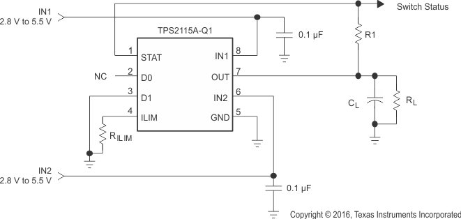
Typical Application

4 Revision History
Changes from * Revision (November 2008) to A Revision
- Changed Applications list Go
- Changed TPS2115A to TPS2155A-Q1 throughout document Go
- Added Device Information table, ESD Ratings table, Feature Description section, Device Functional Modes, Application and Implementation section, Power Supply Recommendations section, Layout section, Device and Documentation Support section, and Mechanical, Packaging, and Orderable Information section. Go
- Changed Continuous output current from 1.5mA to 1.5A in Absolute Maximum Ratings tableGo
- Moved Figure 1 to Switching Characteristics sectionGo
- Moved test circuits from Typical Characteristics to Parameter Measurement Information sectionGo
- Changed info in D0 column with info from D1 column and moved table to Device Functional Modes sectionGo