TPS2291xx Ultra-small, Low On Resistance Load Switch With Controlled Turn-on
1 Features
- Integrated Single Load Switch
- Four Pin Wafer-Chip-Scale Package (Nom)
- 0.9 mm × 0.9 mm, 0.5-mm Pitch, 0.5-mm Height (YZV)
- Input Voltage Range: 1.4 V to 5.5 V
- Low ON-Resistance
- rON = 60 mΩ at VIN = 5 V
- rON = 61 mΩ at VIN = 3.3 V
- rON = 74 mΩ at VIN = 1.8 V
- rON = 84 mΩ at VIN = 1.5 V
- 2-A Maximum Continuous Switch Current
- Low Threshold Control Input
- Controlled Slew-rate
- Under-Voltage Lock Out
- Full-Time Reverse Current Protection
- Quick Output Discharge Transistor (TPS22913B/C Devices)
2 Applications
- Notebook Computer and Ultrabook™
- Tablets and Set-Top-Boxes
- Portable Industrial / Medical Equipment
- Portable Media Players
- Point Of Sale Pins
- GPS Navigation Devices
- Digital Cameras
- Portable Instrumentation
- Smartphones / Wireless Handsets
3 Description
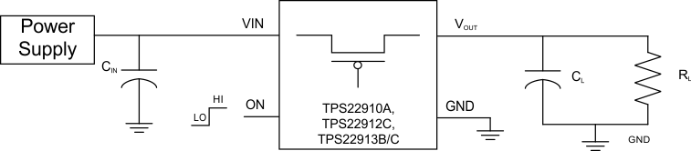
The TPS22910A, TPS22912C, and TPS22913B/C are small, low rON load switches with controlled turn on. The device contains a P-channel MOSFET that can operate over an input voltage range of 1.4 V to 5.5 V. The switch is controlled by an on/off input (ON), which is capable of interfacing directly with low-voltage GPIO control signals.
The TPS22910A, TPS22912C, and TPS22913B/C devices provide reverse current protection in ON and OFF states. An internal reverse voltage comparator disables the power-switch when the output voltage (VOUT) is driven higher than the input voltage (VIN), by VRCP, to quickly (10 µs typ) stop the flow of current towards the input side of the switch. Reverse current protection is always active, even when the power-switch is disabled. Additionally, under-voltage lockout (UVLO) protection turns the switch off if the input voltage is too low.
The TPS22913B/C contains a 150-Ω on-chip load resistor for quick output discharge when the switch is turned off.
This family of devices have various slew rate options to avoid inrush current (see Device Comparison Table for details), are available in an ultra-small, space-saving 4-pin WCSP packages, and are characterized for operation over the free-air temperature range of –40°C to 85°C.
Device Information(1)
| PART NUMBER | PACKAGE | BODY SIZE (NOM) |
|---|---|---|
| TPS22910A | DSBGA (4) | 0.90 mm × 0.90 mm |
| TPS22912C | ||
| TPS22913B | ||
| TPS22913C |
- For all available packages, see the orderable addendum at the end of the datasheet.
4 Simplified Schematic
On-State Resistance vs Input Voltage
5 Revision History
Changes from E Revision (June 2014) to F Revision
- Updated 'ON' pin description in the Pin Functions table. Go
Changes from D Revision (May 2014) to E Revision
- Updated Switching Characteristics table Go
- Updated Typical DC Characteristics section.Go
- Updated Timing Waveforms graphic.Go
- Updated Application Curves section. Go
Changes from C Revision (May 2013) to D Revision
- Combined TPS22910A, TPS22912C, and TPS22913B/C datasheets. Go
6 Device Comparison Table
| DEVICE | rON (typ) at 3.3 V | RISE TIME at 3.3V (typ) |
QUICK OUTPUT DISCHARGE | MAXIMUM OUTPUT CURRENT | ENABLE |
|---|---|---|---|---|---|
| TPS22910A | 61 mΩ | 1 µs | No | 2 A | Active Low |
| TPS22912C | 61 mΩ | 1000 µs | No | 2 A | Active High |
| TPS22913B | 61 mΩ | 66 µs | Yes | 2 A | Active High |
| TPS22913C | 61 mΩ | 660 µs | Yes | 2 A | Active High |

8 Specifications
8.1 Absolute Maximum Ratings
| MIN | MAX | UNIT | |||
|---|---|---|---|---|---|
| VIN | Input voltage range | –0.3 | 6 | V | |
| VOUT | Output voltage range | –0.3 | 6 | V | |
| VON | Input voltage range | –0.3 | 6 | V | |
| IMAX | Maximum continuous switch current | 2 | A | ||
| IPLS | Maximum pulsed switch current, pulse < 300 µs, 2% duty cycle | 2.5 | A | ||
| TA | Operating free-air temperature range | –40 | 85 | °C | |
| TJ | Maximum junction temperature | 125 | °C | ||
| Tstg | Storage temperature range | –65 | 150 | °C | |
8.2 ESD Ratings
| VALUE | UNIT | |||
|---|---|---|---|---|
| V(ESD) | Electrostatic discharge | Human-body model (HBM), per ANSI/ESDA/JEDEC JS-001(1) | ±2000 | V |
| Charged-device model (CDM), per JEDEC specification JESD22-C101(2) | ±1000 | |||
8.3 Recommended Operating Conditions
| MIN | MAX | UNIT | |||
|---|---|---|---|---|---|
| VIN | Input voltage range | 1.4 | 5.5 | V | |
| VON | ON voltage range | 0 | 5.5 | V | |
| VOUT | Output voltage range | VIN | |||
| VIH | High-level input voltage, ON | VIN = 1.4 V to 5.5 V | 1.1 | 5.5 | V |
| VIL | Low-level input voltage, ON | VIN = 3.61 V to 5.5 V | 0.6 | V | |
| VIN = 1.4 V to 3.6 V | 0.4 | V | |||
| CIN | Input capacitor | 1(1) | µF | ||
8.4 Thermal Information
| THERMAL METRIC(1) | TPS22910 | TPS22912 | TPS22913 | UNIT | |
|---|---|---|---|---|---|
| CSP | CSP | CSP | |||
| 4 PINS | 4 PINS | 4 PINS | |||
| RθJA | Junction-to-ambient thermal resistance | 189.1 | 189.1 | 189.1 | °C/W |
| RθJCtop | Junction-to-case (top) thermal resistance | 1.9 | 1.9 | 1.9 | |
| RθJB | Junction-to-board thermal resistance | 36.8 | 36.8 | 36.8 | |
| ψJT | Junction-to-top characterization parameter | 11.3 | 11.3 | 11.3 | |
| ψJB | Junction-to-board characterization parameter | 36.8 | 36.8 | 36.8 | |
8.5 Electrical Characteristics
The electrical characteristics in this section apply to all devices unless otherwise noted. For TPS22910A VON = 0 V where enabled and VON = VIN where disabled. For TPS22912C and TPS22913B/C VON = VIN where enabled and VON = 0 V where disabled. VIN = 1.4 V to 5.5 V, TA = –40ºC to 85ºC (unless otherwise noted)| PARAMETER | TEST CONDITIONS | TA | MIN | TYP | MAX | UNIT | |
|---|---|---|---|---|---|---|---|
| IIN | Quiescent current | IOUT = 0 mA, VIN = 5.25 V, VON = Enabled | Full | 2 | 10 | µA | |
| IOUT = 0 mA, VIN = 4.2 V, VON = Enabled | 2 | 7.0 | |||||
| IOUT = 0 mA, VIN = 3.6 V, VON = Enabled | 2 | 7.0 | |||||
| IOUT = 0 mA, VIN = 2.5 V, VON = Enabled | 0.9 | 5 | |||||
| IOUT = 0 mA, VIN = 1.5 V, VON = Enabled | 0.7 | 5 | |||||
| IIN(off) | Off supply current | RL = 1 MΩ, VIN = 5.25 V, VON = Disabled | Full | 1.2 | 10 | µA | |
| RL = 1 MΩ, VIN = 4.2 V, VON = Disabled | 0.2 | 7.0 | |||||
| RL = 1 MΩ, VIN= 3.6 V, VON = Disabled | 0.1 | 7.0 | |||||
| RL = 1 MΩ, VIN = 2.5 V, VON = Disabled | 0.1 | 5 | |||||
| RL = 1 MΩ, VIN = 1.5 V, VON = Disabled | 0.1 | 5 | |||||
| IIN(Leakage) | Leakage current | VOUT = 0 V, VIN= 5.25 V, VON = Disabled | Full | 1.2 | 10 | µA | |
| VOUT = 0 V, VIN = 4.2 V, VON = Disabled | 0.2 | 7.0 | |||||
| VOUT = 0 V, VIN = 3.6 V, VON = Disabled | 0.1 | 7.0 | |||||
| VOUT = 0 V, VIN = 2.5 V, VON = Disabled | 0.1 | 5 | |||||
| VOUT = 0 V, VIN = 1.5 V, VON = Disabled | 0.1 | 5 | |||||
| rON | On-resistance | VIN = 5.25 V, IOUT = –200 mA | 25°C | 60 | 80 | mΩ | |
| Full | 110 | ||||||
| VIN = 5.0 V, IOUT = –200 mA | 25°C | 60 | 80 | ||||
| Full | 110 | ||||||
| VIN = 4.2 V, IOUT = –200 mA | 25°C | 60 | 80 | ||||
| Full | 110 | ||||||
| VIN = 3.3 V, IOUT = –200 mA | 25°C | 60.7 | 80 | ||||
| Full | 110 | ||||||
| VIN = 2.5 V, IOUT = –200 mA | 25°C | 63.4 | 90 | ||||
| Full | 120 | ||||||
| VIN = 1.8 V, IOUT = –200 mA | 25°C | 74.2 | 100 | ||||
| Full | 130 | ||||||
| VIN = 1.5 V, IOUT = –200 mA | 25°C | 83.9 | 120 | ||||
| Full | 150 | ||||||
| RPD(1) | Output pull down resistance | VIN = 3.3 V, IOUT = 30 mA, VON = 0 | 25°C | 153 | 200 | Ω | |
| UVLO | Under voltage lockout | VIN increasing, VON = 0 V, IOUT = –100 mA |
Full | 1.2 | V | ||
| VIN decreasing, VON = 0 V, RL = 10 Ω | 0.50 | ||||||
| ION | ON input leakage current | VON = 1.4 V to 5.25 V or GND | Full | 1 | µA | ||
| VRCP | Reverse current voltage threshold | TPS22910A, TPS22913B/C | 44 | mV | |||
| TPS22912C | 54 | ||||||
| tDELAY | Reverse current response delay | VIN = 5 V | 10 | µs | |||
| IRCP(leak) | Reverse current protection leakage after reverse current event. | VOUT – VIN > VRCP | 25°C | 0.3 | µA | ||
8.6 Switching Characteristics, Typical
| PARAMETER | TEST CONDITION | TPS22910A | TPS22912C | TPS22913B | TPS22913C | UNIT | |
|---|---|---|---|---|---|---|---|
| VIN = 5 V, TA = 25ºC (unless otherwise noted) | |||||||
| tON | Turn-ON time | RL = 10 Ω, CL = 0.1 µF | 2 | 840 | 76 | 770 | µs |
| tOFF | Turn-OFF time | RL = 10 Ω, CL = 0.1 µF | 5.5 | 6.6 | 6.6 | 6.6 | |
| tR | VOUT rise time | RL = 10 Ω, CL = 0.1 µF | 1 | 912 | 82 | 838 | |
| tF | VOUT fall time | RL = 10 Ω, CL = 0.1 µF | 3 | 3 | 3 | 3 | |
| VIN = 3.3 V, TA = 25ºC (unless otherwise noted) | |||||||
| tON | Turn-ON time | RL = 10 Ω, CL = 0.1 µF | 2.5 | 1147 | 102 | 1048 | µs |
| tOFF | Turn-OFF time | RL = 10 Ω, CL = 0.1 µF | 7 | 8.6 | 8.5 | 8.6 | |
| tR | VOUT rise time | RL = 10 Ω, CL = 0.1 µF | 1 | 1030 | 97 | 980 | |
| tF | VOUT fall time | RL = 10 Ω, CL = 0.1 µF | 3.5 | 3 | 3 | 3 | |
| VIN = 1.5 V, TA = 25ºC (unless otherwise noted) | |||||||
| tON | Turn-ON time | RL = 10 Ω, CL = 0.1 µF | 4.5 | 2513 | 234 | 2344 | µs |
| tOFF | Turn-OFF time | RL = 10 Ω, CL = 0.1 µF | 16.5 | 17.4 | 17 | 18 | |
| tR | VOUT rise time | RL = 10 Ω, CL = 0.1 µF | 2 | 1970 | 244 | 1823 | |
| tF | VOUT fall time | RL = 10 Ω, CL = 0.1 µF | 7 | 6.5 | 6.5 | 6.5 | |
8.7 Typical DC Characteristics
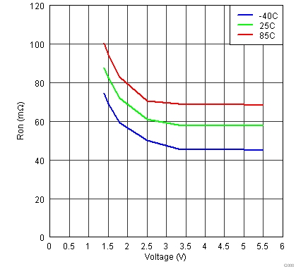
The typical characteristics curves in this section apply to all devices unless otherwise noted.Figure 1. On-State Resistance vs Input Voltage
 Figure 3. TPS22912C and TPS22913B/C On Input Threshold (Active High)

 Figure 7. Input Current, Off vs Input Voltage
 Figure 9. Under Voltage Lockout Response
(IOUT = –100mA)
 Figure 2. TPS22910A On Input Threshold (Active Low)
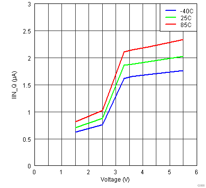 Figure 4. Input Current, Quiescent vs Input Voltage


|
|
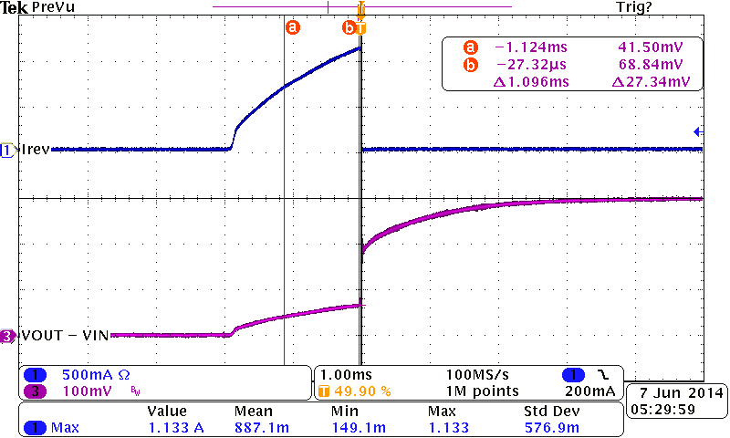 Figure 10. Full-Time Reverse Current Protection
(VIN = 3.0 V, VOUT Ramp up From 3.0 V to 3.3 V)
8.8 Typical AC Characteristics, TPS22910A


 Figure 17. Turn-on Time vs Temperature
 Figure 19. Rise Time vs Input Voltage


 Figure 18. Turn-off Time vs Temperature
8.9 Typical AC Characteristics, TPS22912C


 Figure 26. Turn-on Time vs Temperature
 Figure 28. Rise Time vs Input Voltage


 Figure 27. Turn-off Time vs Temperature
8.10 Typical AC Characteristics, TPS22913B


 Figure 35. Turn-on Time vs Temperature
 Figure 37. Rise Time vs Input Voltage


 Figure 36. Turn-off Time vs Temperature
8.11 Typical AC Characteristics, TPS22913C


 Figure 44. Turn-On Time vs Temperature
 Figure 46. Rise Time vs Input Voltage


 Figure 45. Turn-Off Time vs Temperature