-
TPS23525: –48-V Hot Swap and Dual OR-ing Controller
- 1 Features
- 2 Applications
- 3 Description
- 4 Revision History
- 5 Pin Configuration and Functions
- 6 Specifications
- 7 Parameter Measurement Information
- 8 Detailed Description
-
9 Application and Implementation
- 9.1 Application Information
- 9.2
Typical Application
- 9.2.1 Design Requirements
- 9.2.2
Detailed Design Procedure
- 9.2.2.1 Selecting RSNS
- 9.2.2.2 Selecting Soft Start Setting: CSS and CSS,VEE
- 9.2.2.3 Selecting VDS Switch Over Threshold
- 9.2.2.4 Timer Selection
- 9.2.2.5 MOSFET Selection and SOA Checks
- 9.2.2.6 Input Cap, Input TVS, and OR-ing FET selection
- 9.2.2.7 EMI Filter Consideration
- 9.2.2.8 Under Voltage and Over Voltage Settings
- 9.2.2.9 Choosing RVCC and CVCC
- 9.2.2.10 Power Good Interface to Downstream DC/DC
- 9.2.3 Application Curves
- 10Power Supply Recommendations
- 11Layout
- 12Device and Documentation Support
- 13Mechanical, Packaging, and Orderable Information
- IMPORTANT NOTICE
Package Options
Mechanical Data (Package|Pins)
- PW|16
Thermal pad, mechanical data (Package|Pins)
Orderable Information
TPS23525: –48-V Hot Swap and Dual OR-ing Controller
1 Features
- –10-V to –80-V DC Operation, –200-V Absolute Maximum
- Soft Start Cap Disconnect
- 400-µA Gate Sourcing Current
- Dual Current Limit (based on VDS)
- 25 mV ±4% When Low VDS
- 3 mV ±25% When High VDS
- Programmable UV(±1.5%) and OV (±2%)
- Programmable Hysteresis (±11%)
- Integrated Dual OR-ing Controller
- Regulation: 25 mV ±15 mV
- Fast Turn off: –6 mV ±4 mV
- Retries After Time Out
- 16-Pin TSSOP
2 Applications
- Remote Radio Units
- Baseband Units
- Routers and Switchers
- Small Cells
- –48-V Telecommunications Infrastructure
3 Description
The TPS23525 is an integrated hot swap and dual OR-ing controller that enables high power telecom systems to comply with stringent transient requirements. The 200-V absolute maximum rating makes it easier to survive lightning surge tests (IEC61000-4-5). The soft start cap disconnect allows for the use of smaller hot swap FETs by limiting the inrush current, without hurting the transient response. The 400-µA sourcing current allows fast recovery, which helps to avoid system resets during lightning surge tests. The dual current limit makes it easier to pass brown outs and input steps such as required by the ATIS 0600315.2013. Finally, it offers accurate undervoltage and overvoltage protection with programmable thresholds and hysteresis.
The TPS23525 integrates a dual OR-ing controller, making it ideal for –48-V systems fed by two redundant supplies.
Device Information(1)
| PART NUMBER | PACKAGE | BODY SIZE (NOM) |
|---|---|---|
| TPS23525 | TSSOP (16) | 5.00 mm x 4.40 mm |
- For all available packages, see the orderable addendum at the end of the data sheet.
Simplified Schematic

5 Pin Configuration and Functions
Pin Functions
| PIN | TYPE | DESCRIPTION | |
|---|---|---|---|
| NAME | NO. | ||
| Neg48A | 1 | I | Input to the OR-ing controller for the –48A feed. The TPS23525 will regulate the drop from VEE to Neg48A to 25 mV to mimic an ideal diode. |
| NC | 2 | No connect to space high voltage pins. | |
| GATEB | 3 | O | Gate driver for the OR-ing FET of the -48V_B feed. |
| GATEA | 4 | O | Gate driver for the OR-ing FET of the -48V_A feed. |
| VEE | 5 | GND | This pin corresponds to the IC GND. Kelvin sense to the bottom of RSNS to ensure accurate current limit. |
| SNS | 6 | I | Sense pin, used to measure current and regulate it. Kelvin Sense to RSNS to ensure accurate current limits. |
| GATE | 7 | O | Gate drive for the main hot swap FET. |
| SS | 8 | O | Pin used for soft starting the output. Connect a capacitor (CSS) between the SS pin and -48V_OUT. The dv/dt rate on the -48V_OUT pin is proportional to the gate sourcing current divided by CSS. |
| D | 9 | I | Pin used to sense the drain of the hot swap FET and to program the threshold where the hot swap switches from the CL1 and CL2. Connect a resistor from this pin to the drain of the hot swap FET (also called -48V_OUT) to program the threshold. |
| TMR | 10 | O | Timer pin used to program the duration when the hot swap FET can be in current limit. Program this time by adding a capacitor between the TMR pin and VEE. |
| OV | 11 | I | Input over voltage comparator. Tie a resistor divider to program the threshold where the device turns off due to over voltage event. |
| UVEN | 12 | I | Input under voltage comparator. Tie a resistor divider to program the threshold where the device turns on. |
| VCC | 13 | S | Clamped supply. Tie to RTN through resistor. |
| PGb | 14 | O | Power Good Bar, which is an open drain output that indicated when the power is good and the load can start drawing full power. PGb goes low when the hot swap is fully on and the DC/DC can draw full power. |
| NC | 15 | No connect to space high voltage pins. | |
| Neg48B | 16 | I | Input to the OR-ing controller for the –48B feed. The TPS23525 will regulate the drop from VEE to Neg48B to 25 mV to mimic an ideal diode. |
6 Specifications
6.1 Absolute Maximum Ratings
over operating free-air temperature range (unless otherwise noted)(1)| MIN | MAX | UNIT | ||
|---|---|---|---|---|
| Supply voltage | VVCC (current into VCC <10 mA) | –0.3 | 20 | V |
| Input voltage | VSNS, VOV | –0.3 | 6.5 | V |
| VUVEN, VD(1), VSS(1) | –0.3 | 30 | V | |
| Input voltage | VNeg48A, VNeg48B | -0.3 | 200 | V |
| VNeg48A, VNeg48B through 1-kΩ resistor | –2 | 200 | V | |
| Output voltage | VGATE, VGATEA, VGATEB | –0.3 | VCC | V |
| VTMR | –0.3 | 6.5 | V | |
| Output voltage | VPGb | –0.3 | 200 | V |
| Operating junction temperature, TJ | –40 | 125 | °C | |
| Storage temperature, Tstg | –55 | 150 | °C | |
6.2 ESD Ratings
| VALUE | UNIT | |||
|---|---|---|---|---|
| V(ESD) | Electrostatic discharge | Human-body model (HBM), per ANSI/ESDA/JEDEC JS-001(1) | 1000 | V |
| Charged-device model (CDM), per JEDEC specification JESD22-C101(2) | 500 | |||
6.3 Recommended Operating Conditions
over operating free-air temperature range (unless otherwise noted)| MIN | NOM | MAX | UNIT | ||
|---|---|---|---|---|---|
| VVCC | Supply voltage (current into VCC <10 mA) | 0 | 20 | V | |
| VSNS, VOV | Input voltage | 0 | 5.5 | V | |
| VUVEN, VD(1), VSS(1) | Input voltage | 0 | 18 | V | |
| VNeg48A, VNeg48B | Input voltage, through 1-kΩ resistor | –0.2 | 150 | V | |
| VGATE, VGATEA, VGATEB | Output voltage | 0 | VCC | V | |
| VTMR | Output voltage | 0 | 5.5 | V | |
| VPGb | Output voltage | 0 | 80 | V | |
| CSS | Capacitance | 1 | 200 | nF | |
| RSS | Resistance | 1 | 10 | kΩ | |
| RD | Resistance | 120 | 2,000 | kΩ | |
| RNEG48VA , RNEG48VB | Resistance | 1 | kΩ | ||
6.4 Thermal Information
| THERMAL METRIC(1) | TPS23525 | UNIT | |
|---|---|---|---|
| PW (TSSOP) | |||
| 16 PINS | |||
| RθJA | Junction-to-ambient thermal resistance | 98.4 | °C/W |
| RθJC(top) | Junction-to-case (top) thermal resistance | 31.3 | °C/W |
| RθJB | Junction-to-board thermal resistance | 44.3 | °C/W |
| ψJT | Junction-to-top characterization parameter | 1.8 | °C/W |
| ψJB | Junction-to-board characterization parameter | 43.6 | °C/W |
| RθJC(bot) | Junction-to-case (bottom) thermal resistance | N/A | °C/W |
6.5 Electrical Characteristics
–40°C ≤ TJ ≤125°C, 1.1 mA < IVCC < 10 mA, V(UVEN) = 2 V, V(OV) = V(SNS) = V(D) = 0 V, V(SS) = GATEx = Hi-Z , V(TMR) = 0 V, –1 V < VNEG48Vx < 150 V, ; All pin voltages are relative to VEE (unless otherwise noted)6.6 Switching Characteristics
over operating free-air temperature range (unless otherwise noted)| PARAMETER | TEST CONDITIONS | MIN | TYP | MAX | UNIT | |
|---|---|---|---|---|---|---|
| VCC – Clamped Supply | ||||||
| tID | Insertion Delay | VVCC: 0 V → 10 V, measure delay before VGATE ↑ | 32 | ms | ||
| UVEN | ||||||
| TUV,degl | Deglitch on UVEN | 4 | µs | |||
| OV | ||||||
| TOV,degl | Deglitch on OV | 4 | µs | |||
| SNS | ||||||
| TSNS,FST,RESP | Response time to large over current | VSNS steps from 0 mV to 60 mV. Measure time for GATE to come down. | 300 | ns | ||
| Neg48VA, NEG48VB | ||||||
| TNeg48Vx,FST,RESP | Response time to large reverse current | VNEG48Vx steps from -40 mV to 15 mV. Measure time for GATEx to come down. | 300 | ns | ||
| PGb | ||||||
| tPGb,DEGL | Deglitch of PGb. (raise GATE, measure delay between GATE and PGb) | Power Good ↑ (V(GATE) 0 V → 10 V) Look for PGb ↓ | 1 | ms | ||
| Power Good ↓ (V(GATE) 10 V → 0 V) Look for PGb ↑ | 32 | ms | ||||
6.7 Typical Characteristics
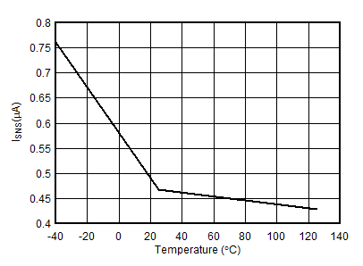
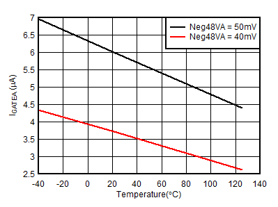
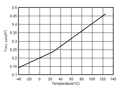
Unless otherwise noted: –40°C ≤ TJ ≤125°C, 1.1 mA < IVCC < 10 mA, V(UVEN) = 2 V, V(OV) = V(SNS) = V(D) = 0 V, V(SS) = GATEx = Hi-Z , V(TMR) = 0 V, –1 V < VNEG48Vx < 150 V , ;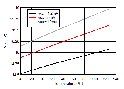
| Ivcc injected into VCC pin |
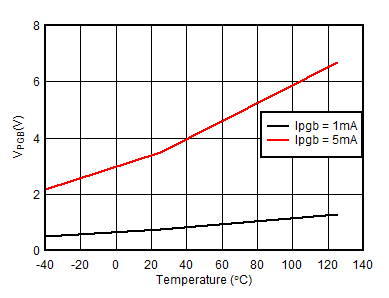
| In Power Good |
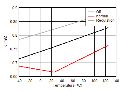
| VVCC = 10 V, Regulation is current limit |
7 Parameter Measurement Information
7.1 Relationship between Sense Voltage, Gate Current, and Timer
The diagram below illustrates the relationship between the VSNS (voltage across RSNS), Gate current, and the timer operation. The diagram is intended to help explain the various parameters in the electrical characteristic table and is not drawn to scale.
Note that IGATE reduces as the sense voltage approaches the current limit threshold and it equals zero at the current limit regulation point. To ensure that the timer always runs when the IC is in regulation the timer starts at a slightly positive IGATE.
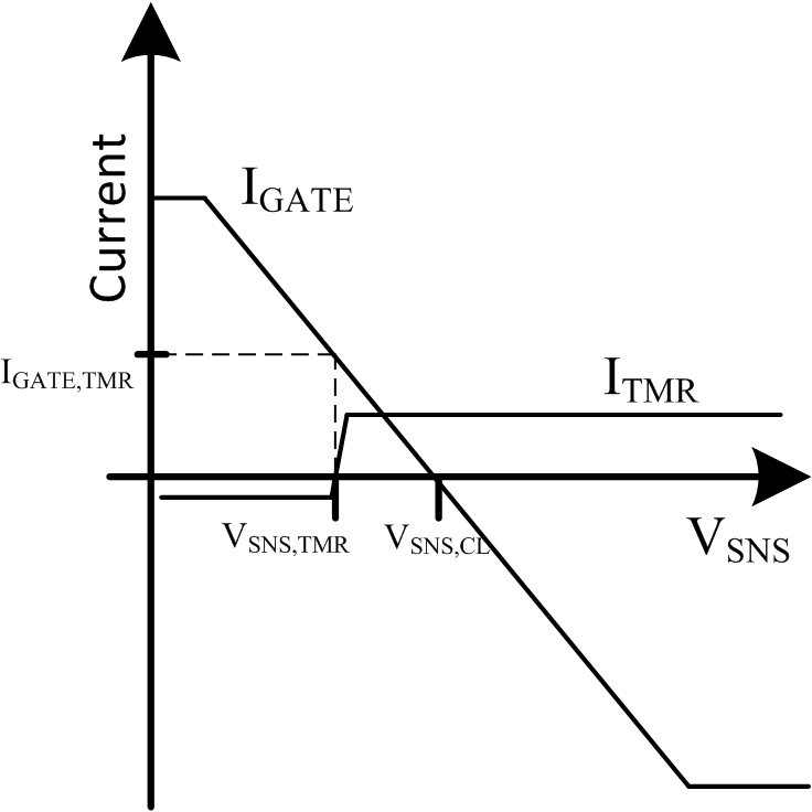 Figure 7. Relationship Between Timer, Gate Current, and Sense Voltage (VGATE = 5 V)
8 Detailed Description
8.1 Overview
The TPS23525 is an integrated hot swap and Dual OR-ing controller that enables high power telecom systems to comply with stringent transient requirements. The soft start cap disconnect allows soft start at start-up and disconnects the soft start cap during normal operation. This allows for the use of smaller hot swap FETs without hurting the transient response. The 400 µA sourcing current allows fast recovery, which helps to avoid system resets during lightning surge tests. The dual current limit makes it easier to pass brown outs and input steps such as required by the ATIS 0600315.2013. Finally, the TPS23525 offers accurate under voltage and over voltage protection with programmable thresholds and hysteresis.
The TPS23525 integrates a dual OR-ing controller, making it ideal for –48 V systems fed by two redundant supplies.The OR-ing controller will turn off if any reverse current is detected.
8.2 Functional Block Diagram
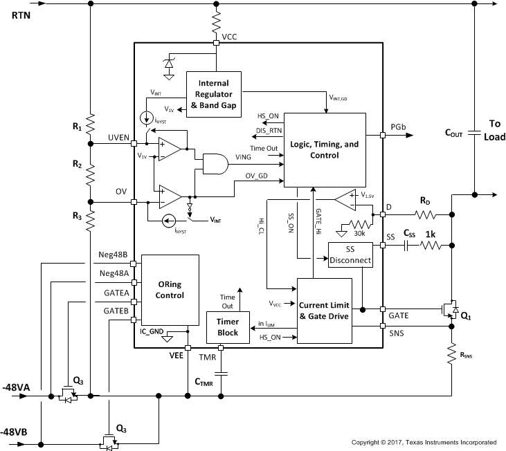
8.3 Feature Description
8.3.1 Current Limit
The TPS23525 utilizes two current limit thresholds:
- ICL1 – also referred to as high current limit threshold, which is used when the VDS of the hot swap FET is low.
- ICL2 – lower current limit threshold, which is used when the VDS of the hot swap FET is high.
This dual level protection scheme ensures that the part has a higher chance of riding out voltage steps and other transients due to the higher current limit at low VDS, while protecting the MOSFET during start into short and hot-short events, by setting a lower current limit threshold for conditions with high VDS. The transition threshold is programmed with a resistor that is connected from the drain of the hot swap FET to the D pin of the TPS23525. The figure below illustrates an example with a ICL1 set to 25 A and ICL2 set to 3 A. Note that compared to a traditional SOA protection scheme this approach allows better utilization of the SOA in the 10 V < VDS. < 40-V range, which is critical in riding through transients and voltage steps.
Note that in both cases the TPS23525 regulated the gate voltage to enforce the current limit. However, this regulation is not very fast and doesn’t offer the best protection against hot-shorts on the output. To protect in this scenario a fast comparator is used, which quickly pulls down the gate in case of severe over current events (2x bigger than VCL1).
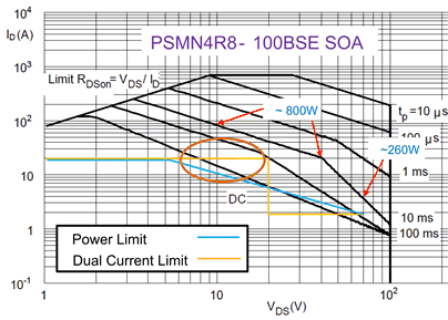 Figure 8. Dual Current Limit vs FET Power Limit
8.3.1.1 Programming the CL Switch-Over Threshold
The VDS threshold when the TPS23525 switches over from ICL1 to ICL2 (VD,SW) can be computed using Equation 1. For example, if a 15-V switch over is desired, RD should be set to 270 kΩ.

8.3.1.2 Programming CL1
The current limit at low VDS (ICL1) of the TPS23525 can be computed using Equation 2 below.

To compute ICL1 for a 1-mΩ sense resistor use Equation 3 below.

8.3.1.3 Programming CL2
The current limit at high VDS (ICL2) of the TPS23525 can be computed using Equation 4 below.

To compute ICL2 for a 1-mΩ sense resistor use Equation 5 below.

8.3.1.4 Computing the Fast Trip Threshold
The fast trip threshold is set to 2x the ICL1 when operating at low VDS and its set to 3x the ICL2 when operating at high VDS.
8.3.2 Soft Start Disconnect
The inrush current into the output capacitor (COUT) can be limited by placing a capacitor between the SS (Soft Start) pin and the drain of the hot swap MOSFET. In that case the inrush current can be computed using equation below.

Note that with most hot swap the CSS pin is tied simply to the gate pin, but this can interfere with performance during normal operation if transients or short circuits are encountered. In addition the CSS capacitor tends to pull up the gate during hot plug and cause shoot through current if it is always tied to the gate. For that reason the TPS23525 has a disconnect switch between the gate pin and the SS pin as well as a discharge resistor. During the initial hot plug and during the insertion delay the switch between SS and GATE is open and SS is being discharged to GND through a resistor. Then during start-up SS and GATE are connected to limit the slew rate. Once in normal operation the SS pin is not tied to GATE and it is not shorted to GND, which prevents it from interfering with the operation during transients.
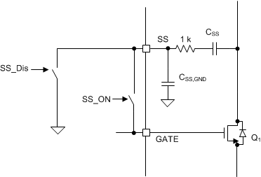 Figure 9. Implementation of SS Disconnect
8.3.3 Timer
Timer is a critical feature in the hot swap, which manages the stress level in the MOSFET. The timer will source and sink current into the timer capacitor as follows:
- Not in current limit: sink 2 µA
- If the part is in current limit and VGATE < VGATE,TH, the timer sources current as follows:
- VD < VD,CL_SW: source 10 µA
- VD > VD,CL_SW: source 50 µA
The TPS23525 times out and shuts down the hot swap as follows.
- If VD < VD,TMR_SW then the hot swap times out when VTMR reaches 1.5 V.
- If VD > VD,TMR_SW then the hot swap times out when VTMR reaches 0.75 V.
The above behavior maximizes the ability of the hot swap to ride out voltage steps, while ensuring that the FET remains safe even if the part can not ride out a voltage step.
A cool down period follows after the part times out. During this time the timer performs the following:
- Discharge CTMR with a 2-µA current source until 0.5 V
- Charge CTMR with a 10-µA current source until it is back to 1.5 V.
- Repeat the above 64 times
- Discharge timer to 0 V.
The part attempts to restart after finishing the above. If the UVEN signal is toggled while the 64 cycles are in progress the part restarts immediately after the 64 cycles are completed.
The timer operates as follows when recovering from POR:
- If VTMR < 0.5 V:
- Proceed to regular startup
- Do not discharge VTMR
- If VTMR > 0.5 V:
- Go through 64 charge/discharge cycles
- Discharge VTMR
- Proceed to startup
The Time Out (TTO) can be computed using the equations below. Note that the time out depends on the VDS of the MOSFET.


8.3.4 OR-ing
The TPS23525 features integrated OR-ing that controls the external MOSFET in a way to emulate an ideal diode. The TPS23525 will regulate the forward drop across the OR-ing FET to 25 mV. This is accomplished by controlling the VGS of the MOSFET. As the current decreases the VGS is also decreased, which effectively increases the RDSON of the MOSFET. This process is regulated with a low gain amplifier that is gate (OR-ing FET) pole compensated. The lower gain helps ensure stability over various operating conditions. The regulating amplifier ensures that there is no DC reverse current.
However, the amplifier is not very fast and thus it is paired with a fast comparator. This comparator quickly turns off the FET if there is significant reverse current detected.
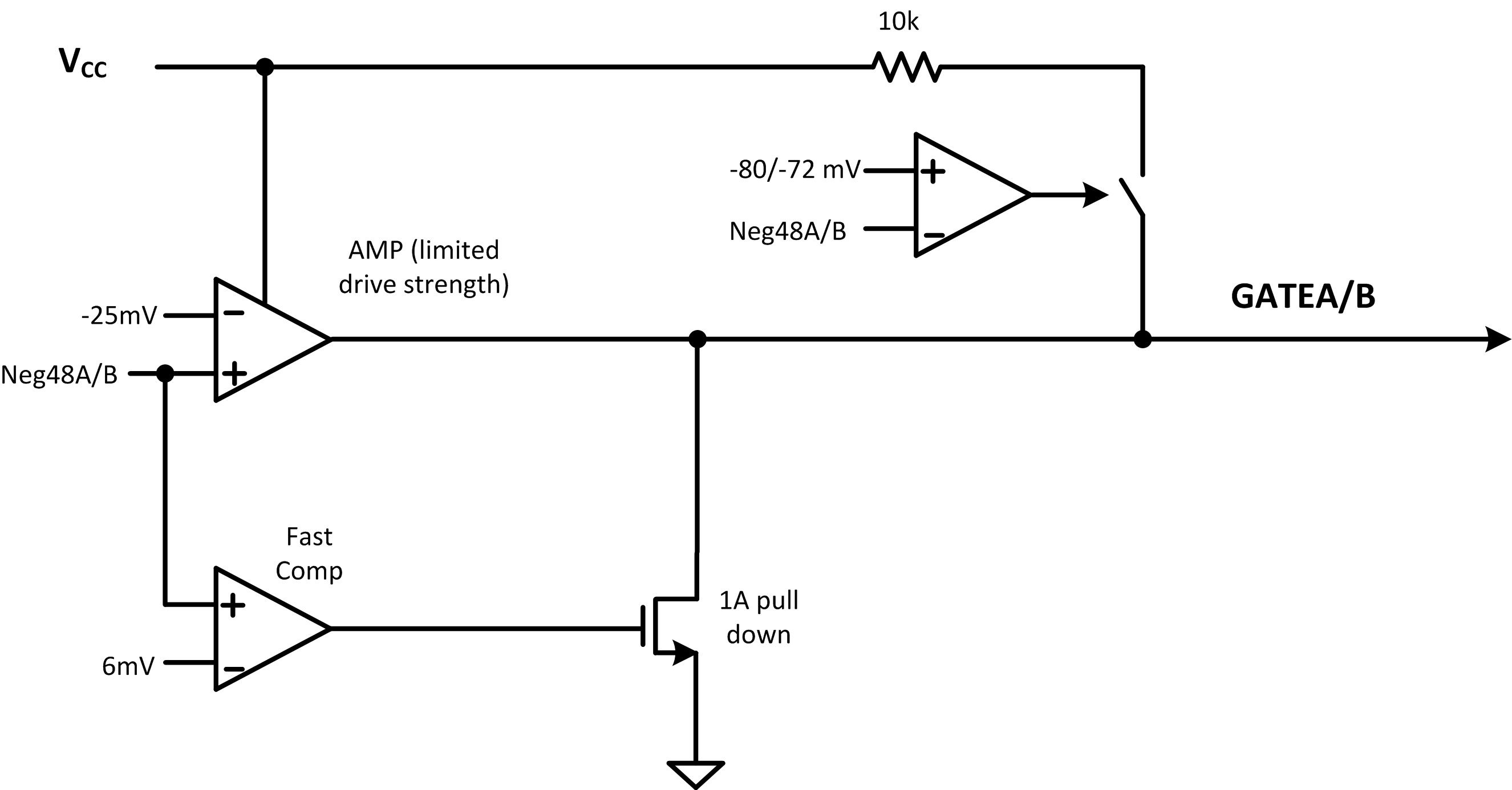 Figure 10. Simplified Diagram of OR-ing Block
8.4 Device Functional Modes
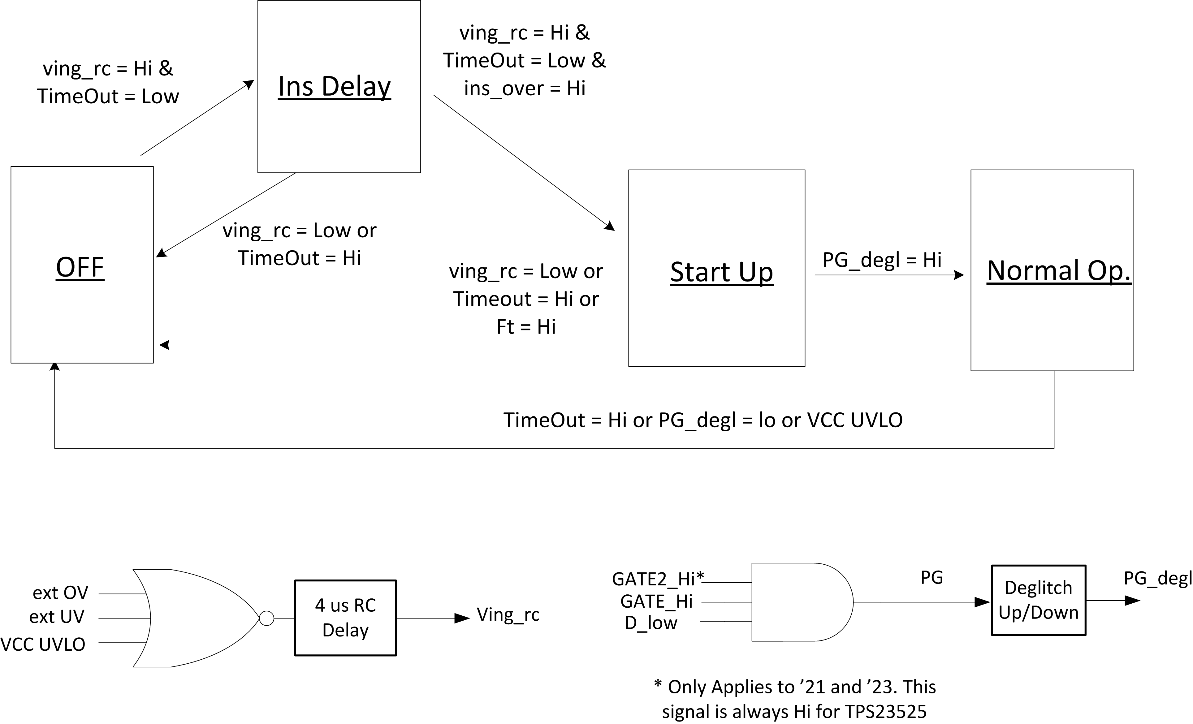 Figure 11. Simplified Hot Swap State Machine
The Figure above shows a simplified state machine of the hot swap controller. It has 4 distinct operating states and the controller switches between these states based on the following signals:
- Ving_rc: This means that both the input voltage is in the right range and the IC has power with Vcc. A 4-µs delay is added for deglitching. If the input voltage is above the OV threshold, input voltage is below the UV threshold, or VCC is below its internal UVLO, Ving_rc will be low.
- TimeOut: This signal comes from the timer block and will be asserted Hi if the IC has timed out due to an over-current condition. This signal is also Hi while the timer is going through the restart cycles. Once the cycles are completed this signal will go Low.
- ins_over: This signal states that the insertion delay has been completed and the hot swap is ready to start-up.
- FT: this is the fast trip signal coming from the fast trip comparator. It goes Hi if an extreme over current event is detected.
- PG: Internal Power good signal. This is high when the hot swap is fully on and the load can draw full power. For PG to be Hi, the GATE has to be Hi and the drain pin needs to be below 0.75 V.
- PG_degl: This is a deglitched version of the PG and is the signal used to move between states and controls the external PGb pin.
8.4.1 OFF State
In this state the hot swap FET is turned off and the controller is waiting to start-up. The controller can be in this state due to any of these scenarios:
- Input voltage is not in the valid range.
- The hot swap is in the cool down state and the timer is going through the retry cycle after a fault condition such as output hot short or over current.
- VCC is below its UVLO threshold and the IC doesn’t have enough power to operate properly.
8.4.2 Insertion Delay State
In this state the hot swap FET is turned off and the controller is waiting for the insertion delay to finish. This allows the input supply to settle after a Hot Plug. If any of the following occur, the controller will be kicked back to the OFF state:
- Input voltage is not in the valid range.
- VCC is below its UVLO threshold and the IC doesn’t have enough power to operate properly.
8.4.3 Start-up State
In this state the controller is turning on and charging the output cap. The operation is set as follows:
- The SS pin is internally connected to the GATE pin to allow for output dv/dt control.
- Lower gate sourcing current is applied to the GATE pin to allow for smaller SS caps.
- The lower current limit setting of VSNS,CL2 and a lower fast trip setting of VSNS,FST2 is used to minimize the MOSFET stress in case of a fault condition.
- Input voltage is not in the valid range.
- The timer times out due to over-current.
- VCC is below its UVLO threshold and the IC doesn’t have enough power to operate properly.
- Fast trip is triggered.
8.4.4 Normal Operation State
In this state the hot swap is fully on and the operation is set as follows:
- The SS pin is disconnected from the GATE pin to improve transient response.
- The full gate sourcing current is used to improve transient response.
- The current limit and fast trip threshold are a function of the D pin to optimize the transient response while protecting the MOSFET.
- • PG_degl goes low.
- The timer times out due to over-current.
- VCC is below its UVLO threshold and the IC doesn’t have enough power to operate properly.