-
TPS54327 3-A Output Single Synchronous Step-Down Switcher With Integrated FET
- 1 Features
- 2 Applications
- 3 Description
- 4 Revision History
- 5 Pin Configuration and Functions
- 6 Specifications
- 7 Detailed Description
- 8 Application and Implementation
- 9 Power Supply Recommendations
- 10Layout
- 11Device and Documentation Support
- 12Mechanical, Packaging, and Orderable Information
- IMPORTANT NOTICE
Package Options
Mechanical Data (Package|Pins)
Thermal pad, mechanical data (Package|Pins)
Orderable Information
TPS54327 3-A Output Single Synchronous Step-Down Switcher With Integrated FET
1 Features
- D-CAP2™ Mode Enables Fast Transient Response
- Low-Output Ripple and Allows Ceramic Output Capacitor
- Wide VIN Input Voltage Range: 4.5 V to 18 V
- Output Voltage Range: 0.76 V to 7 V
- Highly Efficient Integrated FETs Optimized
for Lower Duty Cycle Applications
– 100 mΩ (High-Side) and 70 mΩ (Low-Side) - High Efficiency, Less Than 10 μA at shutdown
- High Initial Bandgap Reference Accuracy
- Adjustable Soft Start
- Prebiased Soft Start
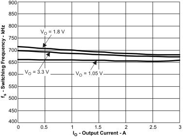
- 700-kHz Switching Frequency (fSW)
- Cycle-By-Cycle Overcurrent Limit
2 Applications
- Wide Range of Applications for Low Voltage System
- Digital TV Power Supply
- High Definition Blu-ray Disc™ Players
- Networking Home Terminal
- Digital Set Top Box (STB)
3 Description
The TPS54327 device is an adaptive on-time D-CAP2™ mode synchronous buck converter. TheTPS54327 enables system designers to complete the suite of various end equipment’s power bus regulators with a cost effective, low component count, low standby current solution. The main control loop for the TPS54327 uses the D-CAP2 mode control which provides a fast transient response with no external compensation components. The TPS54327 also has a proprietary circuit that enables the device to adopt to both low equivalent series resistance (ESR) output capacitors, such as POSCAP or SP-CAP, and ultra-low ESR ceramic capacitors. The device operates from 4.5-V to 18-V VIN input. The output voltage can be programmed between 0.76 V and 7 V. The device also features an adjustable soft start time. The TPS54327 is available in the 8-pin DDA package and 10-pin DRC, and is designed to operate from –40°C to 85°C.
Device Information(1)
| PART NUMBER | PACKAGE | BODY SIZE (NOM) |
|---|---|---|
| TPS54327 | HSOP (8) | 4.89 mm × 3.90 mm |
| VSON (10) | 3.00 mm × 3.00 mm |
- For all available packages, see the orderable addendum at the end of the data sheet.
Simplified Schematic

TPS54327 Transient Response

4 Revision History
Changes from B Revision (January 2012) to C Revision
- Added Pin Configuration and Functions section, ESD Ratings table, Feature Description section, Device Functional Modes, Application and Implementation section, Power Supply Recommendations section, Layout section, Device and Documentation Support section, and Mechanical, Packaging, and Orderable Information section Go
- Removed Ordering Information table Go
Changes from A Revision (October 2011) to B Revision
- Removed (SWIFT™) from the data sheet titleGo
- Added "and 10-pin DRC" to the DESCRIPTIONGo
- Added the DRC-10 Pin package pin outGo
- Changed the VBST(vs SW) MAX value From: 6V to 6.5V in the Abs Max Ratings tableGo
- Changed the VBST(vs SW) MAX value From: 5.7V to 6V in the ROC tableGo
- Changed UVLO MIn Value From: 0.19 V To: 0.17 VGo
- Added Added a conditions statement "VIN = 12 V, TA = 25°C" to the TYPICAL CHARACTERISTICSGo
- Changed Figure 10 title From: 1.05-V, 50-mA to 2-A LOAD TRANSIENT RESPONSE To: 1.05-V, 0-A to 3-A LOAD TRANSIENT RESPONSEGo
- Changed Figure 12 Figure Title From: (IO = 2 A) To: (IO = 3 A)Go
- Changed Figure 13 Figure Title From: (IO = 2 A) To: (IO = 3 A)Go
- Added Figure 17Go
Changes from * Revision (November 2010) to A Revision
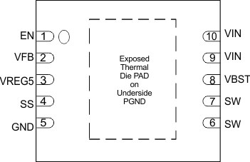
5 Pin Configuration and Functions
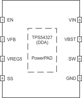
Pin Functions
6 Specifications
6.1 Absolute Maximum Ratings
over operating free-air temperature range (unless otherwise noted) (1)6.2 ESD Ratings
| VALUE | UNIT | |||
|---|---|---|---|---|
| V(ESD) | Electrostatic discharge | Human body model (HBM), per ANSI/ESDA/JEDEC JS-001(1) | ±2000 | V |
| Charged-device model (CDM), per JEDEC specification JESD22-C101(2) | ±500 | |||
6.3 Recommended Operating Conditions
over operating free-air temperature range (unless otherwise noted)6.4 Thermal Information
| THERMAL METRIC(1) | TPS54327 | UNIT | ||
|---|---|---|---|---|
| DDA (HSOP) | DRC (VSON) | |||
| 8 PINS | 10 PINS | |||
| RθJA | Junction-to-ambient thermal resistance | 42.1 | 43.9 | °C/W |
| RθJC(top) | Junction-to-case (top) thermal resistance | 50.9 | 55.4 | °C/W |
| RθJB | Junction-to-board thermal resistance | 31.8 | 18.9 | °C/W |
| ψJT | Junction-to-top characterization parameter | 5 | 0.7 | °C/W |
| ψJB | Junction-to-board characterization parameter | 13.5 | 19.1 | °C/W |
| RθJC(bot) | Junction-to-case (bottom) thermal resistance | 7.1 | 5.3 | °C/W |
6.5 Electrical Characteristics
over operating free-air temperature range VIN = 12 V (unless otherwise noted)| PARAMETER | TEST CONDITIONS | MIN | TYP | MAX | UNIT | |
|---|---|---|---|---|---|---|
| SUPPLY CURRENT | ||||||
| IVIN | Operating - non-switching supply current | VIN current, TA = 25°C, EN = 5 V, VFB = 0.8 V |
800 | 1200 | μA | |
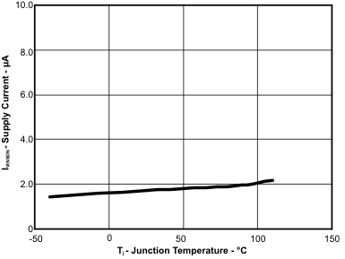
| IVINSDN | Shutdown supply current | VIN current, TA = 25°C, EN = 0 V | 1.8 | 10 | μA | |
| LOGIC THRESHOLD | ||||||
| VENH | EN high-level input voltage | EN | 1.6 | V | ||
| VENL | EN low-level input voltage | EN | 0.45 | V | ||
| VFB VOLTAGE AND DISCHARGE RESISTANCE | ||||||
| VFBTH | VFB threshold voltage | TA = 25°C, VO = 1.05 V, continuous mode | 749 | 765 | 781 | mV |
| IVFB | VFB input current | VFB = 0.8 V, TA = 25°C | 0 | ±0.1 | μA | |
| VREG5 OUTPUT | ||||||
| VVREG5 | VREG5 output voltage | TA = 25°C, 6 V < VIN < 18 V, 0 < IVREG5 < 5 mA |
5.2 | 5.5 | 5.7 | V |
| VLN5 | Line regulation | 6 V < VIN < 18 V, IVREG5 = 5 mA | 25 | mV | ||
| VLD5 | Load regulation | 0 mA < IVREG5 < 5 mA | 100 | mV | ||
| IVREG5 | Output current | VIN = 6 V, VREG5 = 4 V, TA = 25°C | 60 | mA | ||
| MOSFET | ||||||
| RDS(on)h | High-side switch resistance | 25°C, VBST - SW = 5.5 V | 100 | mΩ | ||
| RDS(on)l | Low-side switch resistance | 25°C | 70 | mΩ | ||
| CURRENT LIMIT | ||||||
| Iocl | Current limit | L out = 1.5 μH(1), TA = -20ºC to 85ºC | 3.5 | 4.2 | 5.7 | A |
| THERMAL SHUTDOWN | ||||||
| TSDN | Thermal shutdown threshold | Shutdown temperature (1) | 165 | °C | ||
| Hysteresis (1) | 30 | |||||
| ON-TIME TIMER CONTROL | ||||||
| tON | ON-time | VIN = 12 V, VO = 1.05 V | 150 | ns | ||
| tOFF(MIN) | Minimum OFF-time | TA = 25°C, VFB = 0.7 V | 260 | 310 | ns | |
| SOFT START | ||||||
| ISSC | SS charge current | VSS = 0 V | 1.4 | 2 | 2.6 | μA |
| ISSD | SS discharge current | VSS = 0.5 V | 0.05 | 0.1 | mA | |
| UVLO | ||||||
| UVLO | UVLO threshold | Wakeup VREG5 voltage | 3.45 | 3.75 | 4.05 | V |
| Hysteresis VREG5 voltage | 0.17 | 0.32 | 0.45 | |||
