TPS61042 Constant Current LED Driver
1 Features
- Current Source With Overvoltage Protection
- Input Voltage Range: 1.8 V to 6 V
- Internal 30 V Switch
- Up to 85% Efficiency
- Precise Brightness Control Using PWM Signal or Analog Signal
- Switching Frequency: Up to 1 MHz
- Internal Power MOSFET Switch: 500 mA
- Operates With Small Output Capacitors Down to 100 nF
- Disconnects LEDs During Shutdown
- No Load Quiescent Current: 38 µA Typ
- Shutdown Current: 0.1 µA Typ
- Available in a Small 3 mm × 3 mm QFN Package
2 Applications
- White LED Supply for Backlight/Sidelight Displays
- PDA, Pocket PC, Smart Phones
- Handheld Devices
- Cellular Phones
3 Description
The TPS61042 is a high frequency boost converter with constant current output that drives white LEDs or similar. The LED current is set with the external sense resistor (RS) and is directly regulated by the feedback pin (FB) that regulates the voltage across the sense resistor RS to 252 mV (typ). To control LED brightness, the LED current can be pulsed by applying a PWM (pulse width modulated) signal with a frequency range of 100 Hz to 50 kHz to the control pin (CTRL). To allow higher flexibility, the device can be configured where the brightness can be controlled by an analog signal as well, as described in the application information section. To avoid possible leakage currents through the LEDs during shutdown, the control pin (CTRL) disables the device and disconnects the LEDs from ground. For maximum safety during operation, the output has integrated overvoltage protection that prevents damage to the device in case of a high impedance output (e.g. faulty LED).
Device Information(1)
| PART NUMBER | PACKAGE | BODY SIZE (NOM) |
|---|---|---|
| TPS61042 | SON (8) | 3.00 mm × 3.00 mm |
- For all available packages, see the orderable addendum at the end of the data sheet.
4 Typical Application

5 Revision History
Changes from C Revision (March 2007) to D Revision
- Added Device Information table, Feature Description section, Device Functional Modes, Application and Implementation section, Power Supply Recommendations section, Layout section, Device and Documentation Support section, and Mechanical, Packaging, and Orderable Information section Go
- Added the equation number to all the equations Go
6 Pin Configuration and Functions
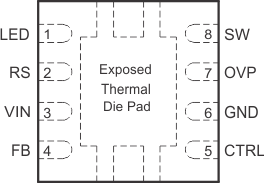
Pin Functions
| PIN | I/O | DESCRIPTION | |
|---|---|---|---|
| NAME | NO. | ||
| CTRL | 5 | I | Combined enable and PWM control pin. If CTRL is constantly pulled high, the device is enabled and the internal LED switch (Q2) is constantly turned on. When CTRL is pulled to GND, the device is disabled. Apply a PWM signal (100 Hz to 50 kHz) to this pin to control the brightness of the LEDs |
| FB | 4 | I | Feedback. FB regulates the LED current through the sense resistor by regulating the voltage across RS to 252 mV. |
| GND | 6 | GND | |
| LED | 1 | I | Input of the LED switch (Q2). Connect the LEDs to this pin. |
| OVP | 7 | I | Overvoltage protection. OVP is connected to the output capacitor of the converter. |
| RS | 2 | O | Output of the internal LED switch. The sense resistor that programs the LED current is connected to RS. |
| SW | 8 | I | Drain of the integrated switch (Q1) |
| VIN | 3 | I | Input supply pin. |
7 Specifications
7.1 Absolute Maximum Ratings
over operating free-air temperature range (unless otherwise noted) (1)| MIN | MAX | UNIT | ||
|---|---|---|---|---|
| V(VIN) | Supply voltages (2) | –0.3 | 7 | V |
| V(Rs) , V(CTRL), V(FB) | Voltages | –0.3 | Vin + 0.3 | V |
| V(SW), V(LED) | Voltages(2) | 30 | V | |
| V(OVP) | Voltage | 30 | V | |
| Continuous power dissipation | See Thermal Information Table | |||
| Operating junction temperature range | –40 | 150 | °C | |
| Storage temperature, TSTG | –65 | 150 | °C | |
7.2 ESD Ratings
| VALUE | UNIT | |||
|---|---|---|---|---|
| V(ESD) | Electrostatic discharge | Human-body model (HBM), per ANSI/ESDA/JEDEC JS-001(1) | ±2000 | V |
| Charged-device model (CDM), per JEDEC specification JESD22-C101(2) | ±750 | |||
7.3 Recommended Operating Conditions
over operating free-air temperature range (unless otherwise noted)| MIN | TYP | MAX | UNIT | ||
|---|---|---|---|---|---|
| VI | Input voltage range | 1.8 | 6 | V | |
| Vs | Output voltage range | VIN | 27.5 | V | |
| VSW | Switch voltage | 30 | V | ||
| I(LED) | Maximum LED switch current | 60 | mA | ||
| L | Inductor(1) | 4.7 | µH | ||
| f | Switching frequency(1) | 1 | MHz | ||
| CI | Input capacitor(1) | 4.7 | µF | ||
| CO | Output capacitor(1) | 100 | nF | ||
| TA | Operating ambient temperature | –40 | 85 | °C | |
| TJ | Operating junction temperature | –40 | 125 | °C | |
7.4 Thermal Information
| THERMAL METRIC(1) | TPS61042 | UNIT | |
|---|---|---|---|
| DRB PACKAGE | |||
| 8 PINS | |||
| RθJA | Junction-to-ambient thermal resistance | 48.6 | °C/W |
| RθJC(top) | Junction-to-case (top) thermal resistance | 66.9 | |
| RθJB | Junction-to-board thermal resistance | 23.8 | |
| ψJT | Junction-to-top characterization parameter | 1.5 | |
| ψJB | Junction-to-board characterization parameter | 23.9 | |
| RθJC(bot) | Junction-to-case (bottom) thermal resistance | 5.2 | |
7.5 Electrical Characteristics
VI = 3.6 V, CTRL= VI, TA = -40°C to + 85°C, typical values are at TA= 25°C (unless otherwise noted)| PARAMETER | TEST CONDITIONS | MIN | TYP | MAX | UNIT | |
|---|---|---|---|---|---|---|
| SUPPLY CURRENT | ||||||
| VI | Input voltage range | 1.8 | 6.0 | V | ||
| I(Q) | Operating quiescent current into VIN | IO = 0 mA, not switching | 38 | 65 | µA | |
| IO(sd) | Shutdown current | CTRL = GND | 0.1 | 1 | µA | |
| VUVLO | Under-voltage lockout threshold | VI falling | 1.5 | 1.7 | V | |
| CTRL | ||||||
| VIH | CTRL high level input voltage | 1.3 | V | |||
| VIL | CTRL low level input voltage | 0.3 | V | |||
| IIkg | CTRL input leakage current | CTRL = GND or VIN | 0.1 | µA | ||
| ton | Minimum CTRL pulse width to enable | CTRL = low to high | 50 | µs | ||
| toff | Minimum CTRL pulse width to disable | CTRL = high to low | 10 | 32 | ms | |
| f(CTRL) | PWM switching frequency applied to CTRL | 0.1 | 50 | kHz | ||
| D(CTRL) | PWM duty cycle applied to CTRL | 1% | 100% | |||
| POWER SWITCH AND CURRENT LIMIT (SW) | ||||||
| VS | Maximum switch voltage | 30 | V | |||
| rds(ON) | MOSFET on-resistance | VI = 3.6 V; I(SW) = 200 mA | 300 | 600 | mΩ | |
| Ilkg | MOSFET leakage current | V(SW) = 28 V | 0.1 | 10 | µA | |
| ILIM | MOFSET current limit | 400 | 500 | 600 | mA | |
| LED SWITCH AND CURRENT LIMIT (LED) | ||||||
| VS | Maximum switch voltage | 30 | V | |||
| rds(ON) | MOSFET on-resistance | VI = 3.6 V; IS = 20 mA | 1 | 2 | Ω | |
| Ilkg | MOSFET leakage current | V(LED)= 28 V | 0.1 | 10 | µA | |
| OUTPUT | ||||||
| VO | Output voltage range | VI | 27.5 | V | ||
| I(FB) | Feedback input bias current(1) | V(FB) = 0.252 V | 100 | nA | ||
| VFB | Feedback trip point voltage | 1.8 V ≤ VI≤ 6 V | 244 | 252 | 260 | mV |
| V(OVP) | Output overvoltage protection | VO rising | 27.5 | 29 | 30 | V |
| Vhys(OVP) | Output overvoltage protection hysteresis | 5 | 7 | V | ||
| I(OVP) | OVP input current | VO = 15 V | 9 | 12 | µA | |
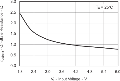
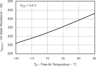
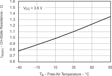
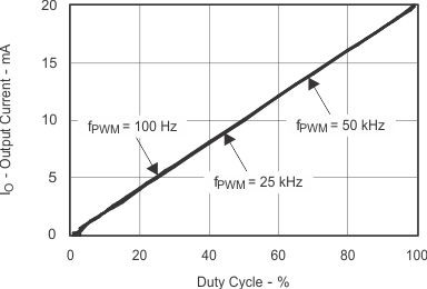
7.6 Typical Characteristics
Table 1. Table of Graphs
| FIGURE | |||
|---|---|---|---|
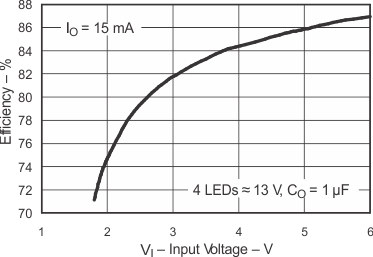
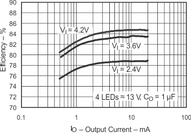
| η | Efficiency | vs LED current | Figure 1 |
| vs Input voltage | Figure 2 | ||
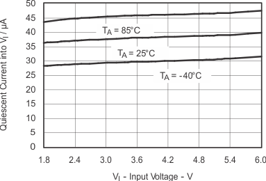
| IQ | Operating Quiescent Current into VIN | vs Input voltage and Temperature | Figure 3 |
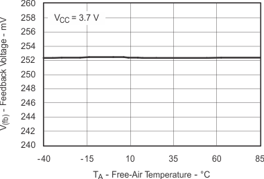
| V(FB) | Feedback voltage | vs Temperature | Figure 4 |
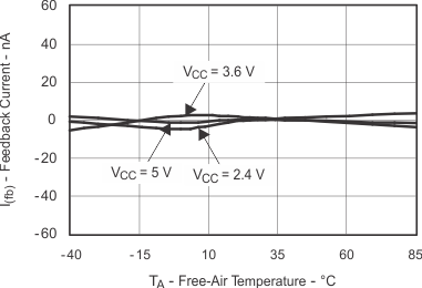
| I(FB) | Feedback current | vs Temperature | Figure 5 |
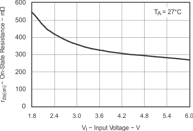
| rds(on) | Main switch Q1 | vs Temperature | Figure 6 |
| vs Input voltage | Figure 7 | ||
| LED switch Q2 | vs Temperature | Figure 8 | |
| vs Input voltage | Figure 9 | ||
| ILED | Average LED current | vs PWM duty cycle on CTRL pin | Figure 10 |
vs Input Voltage and Temperature