TPS6240x 2.25-MHz 400-mA and 600-mA Dual Step-Down Converter In Small 3-mm x 3-mm VSON Package
1 Features
- High Efficiency—Up to 95%
- VIN Range From 2.5 V to 6 V
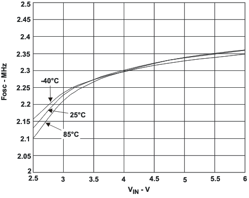
- 2.25-MHz Fixed Frequency Operation
- Output Current of 400 mA and 600 mA
- Adjustable Output Voltage From 0.6V to VIN
- Pin-Selectable Output Voltage Supports Simple Dynamic Voltage Scaling
- EasyScale™ Optional One-Pin Serial Interface
- Power Save Mode at Light Load Currents
- 180° Out-of-Phase Operation
- Output Voltage Accuracy in PWM Mode ±1%
- Typical 32-μA Quiescent Current for Both Converters
- 100% Duty Cycle for Lowest Dropout
- Available in a 10-Pin VSON (3 mm × 3 mm)
2 Applications
- Cell Phones, Smart Phones
- PDAs, Pocket PCs
- OMAP™ and Low-Power DSP Supply
- Portable Media Players
- Digital Radios
- Digital Cameras
3 Description
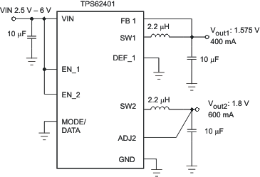
The TPS6240x family of devices are synchronous dual step-down DC-DC converters optimized for battery-powered portable applications. The devices provide two independent output voltage rails powered by 1-cell Li-Ion or 3-cell NiMH/NiCD batteries. The devices are also suitable to operate from a standard 3.3-V or 5-V voltage rail.
With an input voltage range from 2.5 V to 6 V, the TPS6240x is ideal to power portable applications like smart phones, PDAs, and other portable equipment.
With the EasyScale serial interface the output voltages can be modified during operation. The fixed output voltage versions TPS62401, TPS62402, TPS62403, and TPS62404 support one-pin controlled simple Dynamic Voltage Scaling for low-power processors.
The TPS6240x operates at a 2.25-MHz fixed switching frequency and enters the power save mode operation at light load currents to maintain high efficiency over the entire load current range. For low noise applications the devices can be forced into fixed frequency PWM mode by pulling the MODE/DATA pin high. In the shutdown mode, the current consumption is reduced to 1.2 μA, typical. The devices allow the use of small inductors and capacitors to achieve a small solution size.
The TPS6240x is available in a 10-pin leadless package (3-mm × 3-mm VSON)
Device Information(1)
| PART NUMBER | PACKAGE | BODY SIZE (NOM) |
|---|---|---|
| TPS6240x | VSON (10) | 3.00 mm x 3.00 mm |
Simplified Schematic
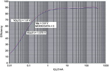
Efficiency vs Output Current
4 Revision History
Changes from E Revision (April 2010) to F Revision
- Added Handling Rating table, Feature Description section, Device Functional Modes, Application and Implementation section, Power Supply Recommendations section, Layout section, Device and Documentation Support section, and Mechanical, Packaging, and Orderable Information sectionGo
Changes from D Revision (February 2006) to E Revision
- Added TPS62404 deviceGo
- Added TPS62404 device to Ordering Information table.Go
- Added TPS62404 device to Addressable Registers table.Go
- Added TPS62404 device to 'Selectable Output Voltages for Converter 1' table.Go
- Added TPS62404 device to 'Selectable Output Voltages for Converter 2' table.Go
- Added TPS62404 device to 'Application Information' section.Go
- Added TPS62404 device efficiency graph (Figure 22).Go
5 Device Options
| TA | PART NUMBER | DEFAULT OUTPUT VOLTAGE(1) | OUTPUT CURRENT | ||
|---|---|---|---|---|---|
| –40 °C to 85 °C | TPS62400 | OUT1 | Adjustable | 400mA | |
| OUT2 | 600mA | ||||
| TPS62401 | OUT1 | Fixed default | DEF_1 = High 1.1V | 400mA | |
| DEF_1 = Low 1.575V | |||||
| OUT2 | Fixed default 1.8V | 600mA | |||
| TPS62402 | OUT1 | Fixed default | DEF_1 = High 1.8V | 400mA | |
| DEF_1 = Low 1.2V | |||||
| OUT2 | Fixed default 3.3V | 600mA | |||
| TPS62403 | OUT1 | Fixed default | DEF_1 = High 1.1V | 400mA | |
| DEF_1 = Low 1.575V | |||||
| OUT2 | Fixed default 2.8V | 600mA | |||
| TPS62404 | OUT1 | Fixed default | DEF_1 = High 1.9V | 400mA | |
| DEF_1 = Low 1.2V | |||||
| OUT2 | Fixed default 3.3V | 600mA | |||
6 Pin Configuration and Functions

Pin Functions
| PIN | I/O | DESCRIPTION | ||
|---|---|---|---|---|
| NAME | NO. | |||
| ADJ2 | 1 | I | Input to adjust output voltage of converter 2. In adjustable version (TPS62400) connect a external resistor divider between VOUT2, this pin and GND to set output voltage between 0.6V and VIN. At fixed output voltage version (TPS62401, TPS62402, TPS62403, TPS62404) this pin MUST be directly connected to the output. If EasyScale Interface is used for converter 2, this pin must be directly connected to the output, too. | |
| DEF_1 | 5 | I | This pin defines the output voltage of converter 1. The pin acts either as analog input for output voltage setting via external resistors (TPS62400), or digital input to select between two fixed default output voltages (TPS62401, TPS62402, TPS62403, TPS62404). | |
| For the TPS62400, an external resistor network needs to be connected to this pin to adjust the default output voltage. | ||||
| Using the fixed output voltage device options this pin selects between two fixed default output voltages, see table ordering information | ||||
| EN1 | 7 | I | Enable Input for Converter1, active high | |
| EN2 | 9 | I | Enable Input for Converter 2, active high | |
| FB1 | 4 | I | Direct feedback voltage sense input of converter 1, connect directly to Vout 1. An internal feed forward capacitor is connected between this pin and the error amplifier. In case of fixed output voltage versions or when the Interface is used, this pin is connected to an internal resistor divider network. | |
| GND | 8 | GND for both converters; connect this pin to the PowerPAD™ | ||
| MODE/DATA | 2 | I/O | This Pin has 2 functions: | |
| 1. | Operation Mode selection: With low level, Power Save Mode is enabled where the device operates in PFM mode at light loads and enters automatically PWM mode at heavy loads. Pulling this PIN to high forces the device to operate in PWM mode over the whole load range. | |||
| 2. | EasyScale™ Interface function: One wire serial interface to change the output voltage of both converters. The pin has an open drain output to provide an acknowledge condition if requested. The current into the open drain output stage may not exceed 500μA. The interface is active if either EN1 or EN2 is high. | |||
| PowerPAD™ | Connect to GND | |||
| SW1 | 6 | I/O | Switch Pin of Converter 1. Connect to Inductor | |
| SW2 | 10 | I/O | Switch Pin of Converter 2. Connect to Inductor. | |
| VIN | 3 | Supply voltage, connect to VBAT, 2.5V to 6V | ||
7 Specifications
7.1 Absolute Maximum Ratings
over operating free-air temperature range (unless otherwise noted)(1)| MIN | MAX | UNIT | |||
|---|---|---|---|---|---|
| Input voltage range on VIN(2) | –0.3 | 7 | V | ||
| Voltage range on EN, MODE/DATA, DEF_1 | –0.3 | VIN +0.3, ≤ 7 | V | ||
| current into MODE/DATA | ≤ 0.5 | mA | |||
| Voltage on SW1, SW2 | –0.3 | 7 | V | ||
| Voltage on ADJ2, FB1 | –0.3 | VIN +0.3, ≤ 7 | V | ||
| TJ(max) | Maximum operating junction temperature | 150 | °C | ||
| TA | Operating ambient temperature range | –40 | 85 | °C | |
7.2 Handling Ratings
| MIN | MAX | UNIT | |||
|---|---|---|---|---|---|
| Tstg | Storage temperature range | –65 | 150 | °C | |
| V(ESD) | Electrostatic discharge(3) | Human body model (HBM), per ANSI/ESDA/JEDEC JS-001, all pins(1) | 1 | kV | |
| Charged device model (CDM), per JEDEC specification JESD22-C101, all pins(2) | 0.5 | ||||
| Machine model | 200 | V | |||
7.3 Recommended Operating Conditions
over operating free-air temperature range (unless otherwise noted)| MIN | NOM | MAX | UNIT | |||
|---|---|---|---|---|---|---|
| VIN | Supply voltage | 2.5 | 6 | V | ||
| VOUT | Output voltage range for adjustable voltage | 0.6 | VIN | V | ||
| TA | Operating ambient temperature | -40 | 85 | °C | ||
| TJ | Operating junction temperature | -40 | 125 | °C | ||
7.4 Thermal Information
| THERMAL METRIC(1) | TPS6240x | UNIT | |
|---|---|---|---|
| VSON | |||
| 10 PINS | |||
| RθJA | Junction-to-ambient thermal resistance | 45.9 | °C/W |
| RθJC(top) | Junction-to-case (top) thermal resistance | 64.3 | |
| RθJB | Junction-to-board thermal resistance | 20.4 | |
| ψJT | Junction-to-top characterization parameter | 1.3 | |
| ψJB | Junction-to-board characterization parameter | 20.6 | |
| RθJC(bot) | Junction-to-case (bottom) thermal resistance | 2.8 | |
7.5 Electrical Characteristics
VIN = 3.6V, VOUT = 1.8V, EN = VIN, MODE = GND, L = 2.2μH, COUT = 20μF, TA = –40°C to 85°C typical values are atTA = 25°C (unless otherwise noted)
| PARAMETER | TEST CONDITIONS | MIN | TYP | MAX | UNIT | ||
|---|---|---|---|---|---|---|---|
| SUPPLY CURRENT | |||||||
| VIN | Input voltage range | 2.5 | 6.0 | V | |||
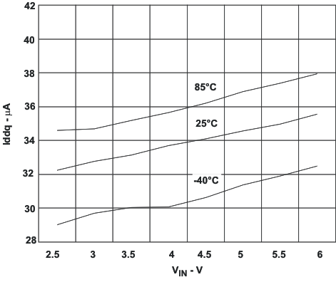
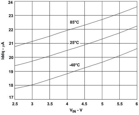
| IQ | Operating quiescent current | One converter, IOUT = 0mA. PFM mode enabled (Mode = 0) device not switching, EN1 = 1 OR EN2 = 1 |
19 | 29 | μA | ||
| Two converter, IOUT = 0mA. PFM mode enabled (Mode = 0) device not switching, EN1 = 1 AND EN2 = 1 |
32 | 48 | μA | ||||
| IOUT = 0mA, MODE/DATA = GND, for one converter, VOUT 1.575V(1) | 23 | μA | |||||
| IOUT = 0mA, MODE/DATA = VIN, for one converter, VOUT 1.575V (1) | 3.6 | mA | |||||
| ISD | Shutdown current | EN1, EN2 = GND, VIN = 3.6V(2) | 1.2 | 3 | μA | ||
| EN1, EN2 = GND, VIN ramped from 0V to 3.6V(3) | 0.1 | 1 | |||||
| VUVLO | Undervoltage lockout threshold | Falling | 1.5 | 2.35 | V | ||
| Rising | 2.4 | ||||||
| ENABLE EN1, EN2 | |||||||
| VIH | High-level input voltage range, EN1, EN2 | 1.2 | VIN | V | |||
| VIL | Low-level input voltage range, EN1, EN2 | 0 | 0.4 | V | |||
| IIN | Input bias current, EN1, EN2 | EN1, EN2 = GND or VIN | 0.05 | 1.0 | μA | ||
| DEF_1 INPUT | |||||||
| VDEF_1H | DEF_1 high level input voltage range | VOUT1 = fixed output voltage option | 0.9 | VIN | V | ||
| VDEF_1L | DEF_1 low level input voltage range | VOUT1 = fixed output voltage option | 0 | 0.4 | V | ||
| IIN | Input bias current DEF_1 | DEF_1 GND or VIN | 0.01 | 1.0 | μA | ||
| MODE/DATA | |||||||
| VIH | High-level input voltage range, MODE/DATA | 1.2 | VIN | V | |||
| VIL | Low-level input voltage range, MODE/DATA | 0 | 0.4 | V | |||
| IIN | Input bias current, MODE/DATA | MODE/DATA = GND or VIN | 0.01 | 1.0 | μA | ||
| VOH | Acknowledge output voltage high | Open drain, via external pullup resistor | VIN | V | |||
| VOL | Acknowledge output voltage low | Open drain, sink current 500μA | 0 | 0.4 | V | ||
| INTERFACE TIMING | |||||||
| tStart | Start time | 2 | μs | ||||
| tH_LB | High time low bit, logic 0 detection | Signal level on MODE/DATA pin is > 1.2V | 2 | 200 | μs | ||
| tL_LB | Low time low bit, logic 0 detection | Signal level on MODE/DATA pin < 0.4V | 2x tH_LB | 400 | μs | ||
| tL_HB | Low time high bit, logic 1 detection | Signal level on MODE/DATA pin < 0.4V | 2 | 200 | μs | ||
| tH_HB | High time high bit, logic 1 detection | Signal level on MODE/DATA pin is > 1.2V | 2x tL_HB | 400 | μs | ||
| TEOS | End of Stream | TEOS | 2 | μs | |||
| tACKN | Duration of acknowledge condition (MODE/DATE line pulled low by the device) | VIN 2.5V to 6V | 400 | 520 | μs | ||
| tvalACK | Acknowledge valid time | 2 | μs | ||||
| ttimeout | Timeout for entering power save mode | MODE/DATA Pin changes from high to low | 520 | μs | |||
| POWER SWITCH | |||||||
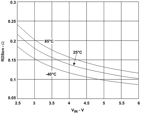
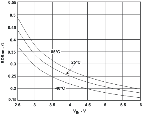
| RDS(ON) | P-Channel MOSFET on-resistance, Converter 1,2 | VIN = VGS = 3.6V | 280 | 620 | mΩ | ||
| ILK_PMOS | P-Channel leakage current | VDS = 6.0V | 1 | μA | |||
| RDS(ON) | N-Channel MOSFET on-resistance Converter 1,2 | VIN = VGS = 3.6V | 200 | 450 | mΩ | ||
| ILK_SW1/SW2 | Leakage current into SW1/SW2 pin | Includes N-Chanel leakage current, VIN = open, VSW = 6.0V, EN = GND(4) |
6 | 7.5 | μA | ||
| ILIMF | Forward Current Limit PMOS and NMOS | OUTPUT 1 | 2.5V ≤ VIN ≤ 6.0V | 0.68 | 0.8 | 0.92 | A |
| OUTPUT 2 | 0.85 | 1.0 | 1.15 | ||||
| TSD | Thermal shutdown | Increasing junction temperature | 150 | °C | |||
| Thermal shutdown hysteresis | Decreasing junction temperature | 20 | °C | ||||
| OSCILLATOR | |||||||
| fSW | Oscillator frequency | 2.5V ≤ VIN ≤ 6V | 2.0 | 2.25 | 2.5 | MHz | |
| OUTPUT | |||||||
| VOUT | Adjustable output voltage range | 0.6 | VIN | V | |||
| Vref | Reference voltage | 600 | mV | ||||
| VOUT (PFM) | DC output voltage accuracy adjustable and fixed output voltage(7) | Voltage positioning active, MODE/DATA = GND, device operating in PFM mode, VIN = 2.5V to 5.0V (5)(8) |
–1.5% | 1.01 VOUT | 2.5% | ||
| VOUT(PWM) | MODE/DATA = GND; device operating in PWM Mode, VIN = 2.5V to 6.0V(8) |
–1% | 0% | 1% | |||
| VIN = 2.5V to 6.0V, Mode/Data = VIN , Fixed PWM operation, 0mA < IOUT1 < 400mA ; 0mA < IOUT2 < 600mA(6) |
–1% | 0% | 1% | ||||
| DC output voltage load regulation | PWM operation mode | 0.5 | %/A | ||||
| tStart up | Start-up time | Activation time to start switching(9) | 170 | μs | |||
| tRamp | VOUT Ramp UP time | Time to ramp from 5% to 95% of VOUT | 750 | μs | |||
7.6 Typical Characteristics