SLVS871D February 2010 – June 2016 TPS62660 , TPS62665
PRODUCTION DATA.
- 1 Features
- 2 Applications
- 3 Description
- 4 Revision History
- 5 Pin Configuration and Functions
- 6 Specifications
- 7 Parameter Measurement Information
- 8 Detailed Description
- 9 Application and Implementation
- 10Power Supply Recommendations
- 11Layout
- 12Device and Documentation Support
- 13Mechanical, Packaging, and Orderable Information
Package Options
Mechanical Data (Package|Pins)
- YFF|6
Thermal pad, mechanical data (Package|Pins)
Orderable Information
1 Features
- 91% Efficiency at 6-MHz Operation
- 31-μA Quiescent Current
- Wide VIN Range from 2.3 V to 5.5 V
- 6-MHz Regulated Frequency Operation
- Best in Class Load and Line Transient
- ±2% Total DC Voltage Accuracy
- Automatic PFM or PWM Mode Switching
- Low Ripple Light-Load PFM Mode
- Fast Turnon Time: < 60-μs Start-Up Time
- Integrated Active Power-Down Sequencing (Optional)
- Current Overload and Thermal Shutdown Protection
- Three Surface-Mount External Components Required (One MLCC Inductor, Two Ceramic Capacitors)
- Complete Sub 1-mm Component Profile Solution
- Total Solution Size <12 mm2
- Available in a 6-Pin NanoFree™ (DSBGA)
2 Applications
- Cell Phones and Smart Phones
- PDAs and Pocket PCs
- Portable Hard Disk Drives
- DC-DC Micro Modules
3 Description
The TPS6266x device is a high-frequency synchronous step-down DC-DC converter optimized for battery-powered portable applications. Intended for low-power applications, the TPS6266x supports up to 1000-mA peak load current, and allows the use of low-cost chip inductor and capacitors.
With a wide input voltage range of 2.3 V to 5.5 V, the device supports applications powered by Li-Ion batteries with extended voltage range. Different fixed voltage output versions are available from 1.2 V to 2.3 V.
The TPS6266x operates at a regulated 6-MHz switching frequency and enters the power-save mode operation at light load currents to maintain high efficiency over the entire load current range.
The PFM mode extends the battery life by reducing the quiescent current to 31 μA (typical) during light load and standby operation. For noise-sensitive applications, the device can be forced into fixed frequency PWM mode by pulling the MODE pin high. In the shutdown mode, the current consumption is reduced to less than 1 μA.
The TPS6266x is available in an 6-pin chip scale package (DSBGA).
Device Information(1)
| PART NUMBER | PACKAGE | BODY SIZE (NOM) |
|---|---|---|
| TPS62660 | DSBGA (6) | 1.30 mm × 0.93 mm |
- For all available packages, see the orderable addendum at the end of the data sheet.
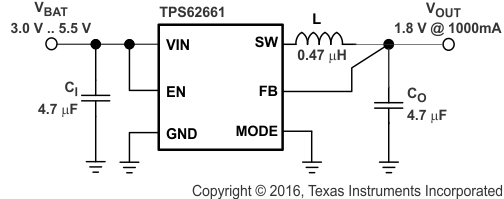
Smallest Solution Size Application

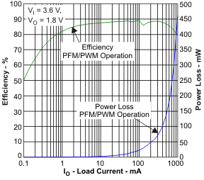
Efficiency vs Load Current
