SLVSCW2A September 2015 – February 2016 TPS657095
PRODUCTION DATA.
- 1 Features
- 2 Applications
- 3 Description
- 4 Revision History
- 5 Pin Configuration and Functions
- 6 Specifications
-
7 Detailed Description
- 7.1 Overview
- 7.2 Functional Block Diagram
- 7.3
Feature Description
- 7.3.1 State Diagram
- 7.3.2 Power-up Timing
- 7.3.3 GPO
- 7.3.4 GPIO
- 7.3.5 LED_EN
- 7.3.6 PWM Dimming
- 7.3.7 Crystal Oscillator and CLKOUT
- 7.3.8 LDOs
- 7.3.9 Undervoltage Lockout
- 7.3.10 Power Up/Power Down Default States
- 7.3.11 Output Voltage Discharge for LDO1 and LDO2
- 7.3.12 Power-Good Status Bits for LDO1 and LDO2
- 7.3.13 Short-Circuit Protection
- 7.3.14 Thermal Shutdown
- 7.3.15 LED Driver
- 7.3.16 4kByte OTP Memory
- 7.4 Device Functional Modes
- 7.5 Programming
- 7.6
Register Map
- 7.6.1 DEV_AND_REV_ID Register Address: 00h
- 7.6.2 OTP_REV Register Address: 01h
- 7.6.3 GPIO_CTRL Register Address: 02h
- 7.6.4 PWM_OSC_CNTRL Register Address: 03h
- 7.6.5 ISINK_CURRENT Register Address: 04h
- 7.6.6 LDO_CTRL Register Address: 05h
- 7.6.7 LDO1_VCTRL Register Address: 06h
- 7.6.8 LDO2_VCTRL Register Address: 07h
- 7.6.9 PWM_DUTY_THR_L Register Address: 08h
- 7.6.10 PWM_DUTY_THR_H Register Address: 09h
- 7.6.11 RESERVED Register Address: 0Ah
- 7.6.12 PWM_DUTY_L Register Address: 0Bh
- 7.6.13 PWM_DUTY_H Register Address: 0Ch
- 7.6.14 RESERVED Register Address: 0Dh
- 7.6.15 SPARE Register Address: 0Eh
- 7.6.16 4K_OTP_PASSWORD Register Address: 0Fh
- 8 Application and Implementation
- 9 Power Supply Recommendations
- 10Layout
- 11Device and Documentation Support
- 12Mechanical, Packaging, and Orderable Information
Package Options
Mechanical Data (Package|Pins)
- YFF|16
Thermal pad, mechanical data (Package|Pins)
Orderable Information
1 Features
- Two 100mA LDOs
- Output Voltage Accuracy ±1.5%
- VIN Range From 3.7V to 6V
- LED Driver with PWM Dimming
- 1 GPO
- 1 GPIO
- I2C™ Interface
- 4KByte User OTP memory
- Available in 16-Ball DSBGA with 0.4mm Pitch
2 Applications
- Laptops
- Detachables
- Tablets
- Monitors
- Smartphones
3 Description
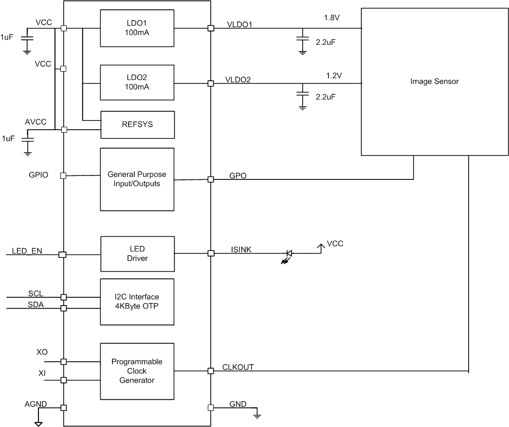
The TPS657095 is a power management unit targeted for embedded camera modules or other portable low power consumer end equipments. It contains two LDOs enabled by the I2C™ Interface, a PWM-dimmable current sink for driving one LED, one general purpose output (GPO), a programmable clock generator and 4K Byte of User OTP memory. The operation of the device is disabled if the input voltage supply is below the internal undervoltage lockout.
The device comes in a 16-ball die-size ball grid array package (DSBGA) with 0.4mm ball pitch.
Device Information(1)
| PART NUMBER | PACKAGE | BODY SIZE (NOM) |
|---|---|---|
| TPS657095 | DSBGA (16) | 1.70 mm x 1.70 mm |
- For all available packages, see the orderable addendum at the end of the datasheet.
space
Application Circuit
