SLUSC66E March 2015 – February 2017 UCD3138A
PRODUCTION DATA.
- 1 Device Overview
- 2 Device Comparison
- 3 Pin Configuration and Functions
- 4 Specifications
- 5 Parametric Measurements Information
-
6 Detailed Description
- 6.1 Overview
- 6.2 ARM Processor
- 6.3 Memory
- 6.4 System Module
- 6.5
Feature Description
- 6.5.1 Sync FET Ramp and IDE Calculation
- 6.5.2 Automatic Mode Switching
- 6.5.3 DPWMC, Edge Generation, IntraMux
- 6.5.4 Filter
- 6.5.5 Communication Ports
- 6.5.6 Miscellaneous Analog
- 6.5.7 Package ID Information
- 6.5.8 Brownout
- 6.5.9 Global I/O
- 6.5.10 Temperature Sensor Control
- 6.5.11 I/O Mux Control
- 6.5.12 Current Sharing Control
- 6.5.13 Temperature Reference
- 7 Device Functional Modes
- 8 Application and Implementation
- 9 Power Supply Recommendations
- 10Layout
- 11Device and Documentation Support
- 12Mechanical Packaging and Orderable Information
Package Options
Mechanical Data (Package|Pins)
Thermal pad, mechanical data (Package|Pins)
Orderable Information
1 Device Overview
1.1 Features
- Digital Control of up to 3 Independent Feedback Loops
- Dedicated PID-Based Hardware
- 2-Pole, 2-Zero Configurable
- Nonlinear Control
- Soft-Start and Soft-Stop with and without Prebias
- Fast Input Voltage Feed Forward Hardware
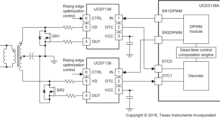
- Synchronous Rectifier Dead Time Optimization Peripheral to Use with UCD7138 Synchronous Rectifier Driver
- Up to 16 MHz Error Analog-to-Digital Converter (EADC)
- Configurable Resolution as Small as 1 mV/LSB
- Automatic Resolution Selection
- Up to 8× Oversampling
- Hardware-Based Averaging (up to 8×)
- 10-Bit Effective DAC With 4 Bits of Dither
- Adaptive Sample Trigger Positioning
- Up to 8 High-Resolution Digital Pulse Width Modulated (DPWM) Outputs
- 250-ps Pulse Width Resolution
- 4-ns Frequency and Phase Resolution
- Adjustable Phase-Shift Between Outputs
- Adjustable Dead-band Between Pairs
- Cycle-by-Cycle Duty Cycle Matching
- Up to 2-MHz Switching Frequency
- Configurable PWM Edge Movement
- Trailing Modulation
- Leading Modulation
- Triangular Modulation
- Configurable Feedback Control
- Voltage Mode
- Average Current Mode
- Peak Current Mode Control
- Constant Current
- Constant Power
- Configurable Modulation Methods
- Frequency Modulation
- Phase-Shift Modulation
- Pulse Width Modulation
- Fast, Automatic, and Smooth Mode Switching
- Frequency Modulation and PWM
- Phase-Shift Modulation and PWM
- Frequency Modulation and Phase-Shift Modulation
- High Efficiency and Light Load Management
- Burst Mode
- Ideal Diode Emulation
- Synchronous Rectifier Soft On/Off
- Low IC Standby Power
- Primary Side Voltage Sensing
- Copper Trace Current Sensing
- Flux and Phase Current Balancing
- Current Share Bus Support
- Average or Master and Slave
- Feature Rich Fault Protection Options
- 7 High-Speed Analog Comparators
- Cycle-by-Cycle Current Limiting
- Programmable Fault
- External Fault Capability
- 10 Digital Comparators
- Programmable Blanking Time
- Synchronization of DPWM Waveforms Between Multiple UCD3138A devices
-
14-Channel, 12-Bit, 267-ksps General-Purpose ADC
- Programmable Averaging Filters
- Dual Sample and Hold
- Internal Temperature Sensor
- Fully Programmable High-Performance 31.25-MHz, 32-Bit ARM7TDMI-S™ Processor
- Communication Peripherals
- PMBus
- 1 UART
- UART Auto-baud Rate Adjustment
- Timer Capture with Selectable Input Pins
- Up to 5 Additional General Purpose Timers
- Built In Watchdog: BOD and POR
- 64-Pin QFN and 40-Pin QFN Package
- Operating Temperature: –40°C to +125°C
- Debug Interface
- Code Composer Studio™ with JTAG Interface
- Fusion Digital Power™ Designer GUI Support
1.2 Applications
- Power Supplies and Telecom Rectifiers
- Power Factor Correction
- Isolated DC-DC Modules
1.3 Description
The UCD3138A is a digital power supply controller from Texas Instruments offering superior levels of integration and performance in a single-chip solution. The flexible nature of the UCD3138A makes it suitable for a wide variety of power conversion applications. In addition, multiple peripherals inside the device have been specifically optimized to enhance the performance of AC-DC and isolated DC-DC applications and reduce the solution component count in the IT and network infrastructure space.
The UCD3138A controller is a fully programmable solution offering customers complete control of their application, along with ample ability to differentiate their solution. At the same time, TI is committed to simplifying our customers' development effort by offering best-in-class development tools, including application firmware, Code Composer Studio™ software development environment, and TI’s power development GUI which lets customers configure and monitor key system parameters.
At the core of the UCD3138A controller are the digital control loop peripherals, also known as Digital Power Peripherals (DPPs). Each DPP implements a high-speed digital control loop consisting of a dedicated error analog-to-digital converter (EADC), a PID-based 2-pole-2-zero digital compensator and DPWM outputs with 250-ps pulse width resolution. The device also contains a 12-bit, 267-ksps general-purpose ADC with up to 14 channels, timers, interrupt control, PMBus, and UART communications ports. The device is based on a 32-bit ARM7TDMI-S RISC microcontroller that performs real-time monitoring, configures peripherals, and manages communications. The ARM microcontroller executes its program out of programmable flash memory as well as on-chip RAM and ROM.
In addition to the DPP, specific power management peripherals have been added to enable high efficiency across the entire operating range, high integration for increased power density, reliability, and lowest overall system cost and high flexibility with support for the widest number of control schemes and topologies. Such peripherals include: light load burst mode, synchronous rectification, automatic mode switching, input voltage feed forward, copper trace current sense, ideal diode emulation, constant current constant power control, synchronous rectification soft on and off, peak current mode control, flux balancing, secondary side input voltage sensing, high-resolution current sharing, hardware-configurable soft-start operation with pre-bias, as well as several other features. The device optimizes topology support for voltage mode and peak current mode controlled phase-shifted full bridge, single and dual phase PFC, bridge-less PFC, hard-switched full bridge and half bridge, and LLC half bridge and full bridge.
The UCD3139A is a functional variant of the UCD3138A Digital Power Controller that includes significant improvements over the UCD3138 device For a description of the complete changes made in the UCD3138A, refer to UCD3138A Migration Guide.
Device Information(1)
| DEVICE NUMBER | PACKAGE DRAWING | PACKAGE TYPE | BODY SIZE |
|---|---|---|---|
| UCD3138A | RGC | VQFN (64) | 9.00 mm × 9.00 mm |
| RJA | VQFN (40)(3) | 6.00 mm × 6.00 mm | |
| RMH | WQFN (40) | 6.00 mm × 6.00 mm |
- For all available packages, see the orderable addendum at the end of the datasheet.
- 40-pin 6 x 6 x 0.75 mm ultra-thin QFN with corner anchors optimized for IPC9592A Temperature Cycle Testing.
- Recommended for new 40-pin designs, optimized for improved performance under temperature cycling test for board level reliability (BLR).
1.4 Functional Block Diagram
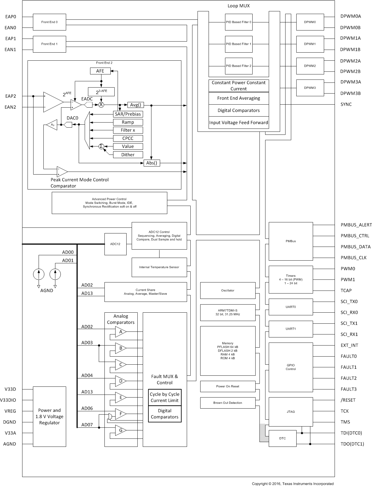
Figure 1-1 shows a functional block diagram of the device.
 Figure 1-1 Functional Block Diagram
