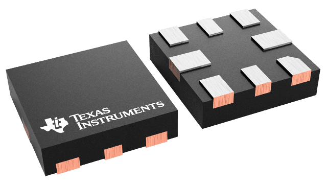
Packaging information
| Package | Pins X2QFN (RUG) | 8 |
| Operating temperature range (°C) -40 to 125 |
| Package qty | Carrier 3,000 | LARGE T&R |
Features for the ADS7040
- Industry’s First SAR ADC with Nanowatt Power Consumption:
- 171 µW at 1 MSPS with 1.8-V AVDD
- 555 µW at 1 MSPS with 3-V AVDD
- 56 µW at 100 kSPS with 3-V AVDD
- Less than 1 µW at 1 kSPS with 3-V AVDD
- Industry’s Smallest SAR ADC:
- X2QFN-8 Package with 2.25-mm2 Footprint
- 1-MSPS Throughput with Zero Data Latency
- Wide Operating Range:
- AVDD: 1.65 V to 3.6 V
- DVDD: 1.65 V to 3.6 V (Independent of AVDD)
- Temperature Range: –40°C to 125°C
- Excellent Performance:
- 8-Bit Resolution with NMC
- ±0.5-LSB (Max) INL, ±0.4-LSB (Max) DNL
- 49 dB SNR
- –70-dB THD
- Unipolar Input Range: 0 V to AVDD
- Integrated Offset Calibration
- SPI™-Compatible Serial Interface: 12 MHz
- JESD8-7A Compliant Digital I/O
Description for the ADS7040
The ADS7040 is a 8-bit, 1-MSPS, analog-to-digital converter (ADC). The device supports a wide analog input voltage range (1.65 V to 3.6 V) and includes a capacitor-based, successive-approximation register (SAR) ADC with an inherent sample-and-hold circuit. The SPI-compatible serial interface is controlled by the CS and SCLK signals. The input signal is sampled with the CS falling edge and SCLK is used for conversion and serial data output. The device supports a wide digital supply range (1.65 V to 3.6 V), enabling direct interface to a variety of host controllers. The ADS7040 complies with the JESD8-7A standard for a normal DVDD range (1.65 V to 1.95 V).
The ADS7040 is available in 8-pin, miniature, leaded, and X2QFN packages and is specified for operation from –40°C to 125°C. Miniature form-factor and extremely low-power consumption make this device suitable for space-constrained, battery-powered applications.
