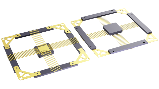
Packaging information
| Package | Pins CFP (HFG) | 36 |
| Operating temperature range (°C) 25 to 25 |
| Package qty | Carrier 10 | JEDEC TRAY (5+1) |
Features for the CDCLVP111-SP
- Distributes One Differential Clock Input Pair LVPECL to 10 Differential LVPECL
- Fully Compatible With LVECL and LVPECL
- Supports a Wide Supply Voltage Range From 2.375V to 3.8V
- Selectable Clock Input Through CLK_SEL
- Low-Output Skew (Typical 15ps) for
Clock-Distribution Applications
- Additive Jitter Less Than 1ps
- Propagation Delay Less Than 355ps
- Open Input Default State
- LVDS, CML, SSTL input Compatible
- VBB Reference Voltage Output for Single-Ended Clocking
- Frequency Range From DC to 3.5GHz
- Supports Defense, Aerospace, and Medical Applications
- Controlled Baseline
- One Assembly and Test Site
- One Fabrication Site
- Available in Military (–55°C to 125°C) Temperature Range (1)
- Extended Product Life Cycle
- Extended Product-Change Notification
- Product Traceability
(1)Custom temperature ranges available.
Description for the CDCLVP111-SP
The CDCLVP111-SP clock driver distributes one differential clock pair of LVPECL input, (CLK0, CLK1) to ten pairs of differential LVPECL clock (Q0, Q9) outputs with minimum skew for clock distribution. The CDCLVP111-SP can accept two clock sources into an input multiplexer. The CDCLVP111-SP is specifically designed for driving 50Ω transmission lines. When an output pin is not used, leaving the pin open is recommended to reduce power consumption. If only one of the output pins from a differential pair is used, the other output pin must be identically terminated to 50Ω.
The VBB reference voltage output is used if single-ended input operation is required. In this case, the VBB pin must be connected to CLK0 and bypassed to GND using a 10nF capacitor.
For high-speed performance, the differential mode is strongly recommended.
The CDCLVP111-SP is characterized for operation from –55°C to 125°C.