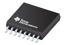
Packaging information
| Package | Pins SOIC (DW) | 16 |
| Operating temperature range (°C) -40 to 125 |
| Package qty | Carrier 40 | TUBE |
Features for the ISO5852S-Q1
- Qualified for Automotive Applications
- AEC-Q100 Qualified With the Following Results:
- Device Temperature Grade 1: –40°C to +125°C Ambient Operating Temperature Range
- Device HBM Classification Level 3A
- Device CDM Classification Level C6
- 100-kV/μs Minimum Common-Mode Transient Immunity (CMTI) at VCM = 1500 V
- Split
Outputs to Provide 2.5-A Peak Source and
5-A Peak Sink Currents - Short Propagation Delay: 76 ns (Typ),
110 ns (Max) - 2-A Active Miller Clamp
- Output Short-Circuit Clamp
- Soft Turn-Off (STO) during Short Circuit
- Fault Alarm upon Desaturation Detection is Signaled on FLT and Reset Through RST
- Input and Output Undervoltage Lockout (UVLO) with Ready (RDY) Pin Indication
- Active Output Pulldown and Default Low Outputs with Low Supply or Floating Inputs
- 2.25-V to 5.5-V Input Supply Voltage
- 15-V to 30-V Output Driver Supply Voltage
- CMOS Compatible Inputs
- Rejects Input Pulses and Noise Transients Shorter Than 20 ns
- Isolation Surge Withstand Voltage 12800-VPK
- Safety-Related Certifications:
- 8000-VPK VIOTM and 2121-VPK VIORM Reinforced Isolation per DIN V VDE V 0884-10 (VDE V 0884-10):2006-12
- 5700-VRMS Isolation for 1 Minute per UL 1577
- CSA Component Acceptance Notice 5A, IEC 60950–1 and IEC 60601–1 End Equipment Standards
- TUV Certification per EN 61010-1 and EN 60950-1
- GB4943.1-2011 CQC Certification
- All Certifications Complete per UL, VDE, CQC, TUV and Planned for CSA
All trademarks are the property of their respective owners.
Description for the ISO5852S-Q1
The ISO5852S-Q1 device is a 5.7-kVRMS, reinforced isolated gate driver for IGBTs and MOSFETs with split outputs, OUTH and OUTL, providing 2.5-A source and 5-A sink current. The input side operates from a single 2.25-V to 5.5-V supply. The output side allows for a supply range from minimum 15 V to maximum 30 V. Two complementary CMOS inputs control the output state of the gate driver. The short propagation time of 76 ns provides accurate control of the output stage.
An internal desaturation (DESAT) fault detection recognizes when the IGBT is in an overcurrent condition. Upon a DESAT detect, a mute logic immediately blocks the output of the isolator and initiates a soft-turnoff procedure which disables the OUTH pin and pulls the OUTL pin to low over a time span of 2 μs. When the OUTL pin reaches 2 V with respect to the most-negative supply potential, VEE2, the gate-driver output is pulled hard to the VEE2 potential, turning the IGBT immediately off.
When desaturation is active, a fault signal is sent across the isolation barrier, pulling the FLT output at the input side low and blocking the isolator input. Mute logic is activated through the soft-turnoff period. The FLT output condition is latched and can be reset only after the RDY pin goes high, through a low-active pulse at the RST input.
When the IGBT is turned off during normal operation with a bipolar output supply, the output is hard clamp to VEE2. If the output supply is unipolar, an active Miller clamp can be used, allowing Miller current to sink across a low-impedance path which prevents the IGBT from dynamic turnon during high-voltage transient conditions.
The readiness for the gate driver to be operated is under the control of two undervoltage-lockout circuits monitoring the input-side and output-side supplies. If either side has insufficient supply, the RDY output goes low, otherwise this output is high.
The ISO5852S-Q1 device is available in a 16-pin SOIC package. Device operation is specified over a temperature range from –40°C to +125°C ambient.
For all available packages, see the orderable addendum at the end of the data sheet.