Packaging information
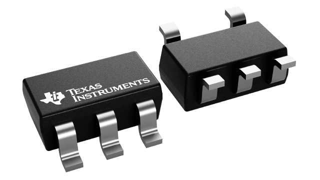
| Package | Pins SOT-23 (DBV) | 5 |
| Operating temperature range (°C) -40 to 125 |
| Package qty | Carrier 1,000 | SMALL T&R |
Features for the LMV796-Q1
- Input Referred Voltage Noise 5.8 nV/√Hz
- Input Bias Current 100 fA
- Unity Gain Bandwidth 17 MHz
- Supply Current per
Channel
- LMV796/LMV796Q 1.15 mA
- LMV797 1.30 mA
- Rail-to-Rail Output Swing
- @ 10 kΩ Load 25 mV from Rail
- @ 2 kΩ Load 45 mV from Rail
- Guaranteed 2.5V and 5.0V Performance
- Total Harmonic Distortion 0.01% @ 1kHz, 600Ω
- Temperature Range −40°C to 125°C
- LMV796Q is an Automotive Grade Product that is AEC-Q100 Grade 1 Qualified and is Manufactured on an Automotive Grade Flow.
(Typical 5V Supply, Unless Otherwise Noted)
All trademarks are the property of their respective owners.
Description for the LMV796-Q1
The LMV796/LMV796Q (Single) and the LMV797 (Dual) low noise, CMOS input operational amplifiers offer a low input voltage noise density of 5.8 nV/√Hz while consuming only 1.15 mA (LMV796/LMV796Q) of quiescent current. The LMV796/LMV796Q and LMV797 are unity gain stable op amps and have gain bandwidth of 17 MHz. The LMV796/LMV796Q/ LMV797 have a supply voltage range of 1.8V to 5.5V and can operate from a single supply. The LMV796/LMV796Q/LMV797 each feature a rail-to-rail output stage capable of driving a 600Ω load and sourcing as much as 60 mA of current.
The LMV796/LMV796Q family provides optimal performance in low voltage and low noise systems. A CMOS input stage, with typical input bias currents in the range of a few femtoAmperes, and an input common mode voltage range, which includes ground, make the LMV796/LMV796Q and the LMV797 ideal for low power sensor applications.
The LMV796/LMV796Q/LMV797 are manufactured using TI’s advanced VIP50 process. The LMV796/ LMV796Q are offered in 5–pin SOT-23 package. The LMV797 is offered in 8–pin VSSOP package.