Packaging information
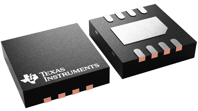
| Package | Pins WSON (DRG) | 8 |
| Operating temperature range (°C) -40 to 125 |
| Package qty | Carrier 3,000 | LARGE T&R |
Features for the LP2951-Q1
- AEC-Q100 qualified for automotive applications:
- Temperature grade 1: −40°C to +125°C, TA
- Temperature grade 1: −40°C to +125°C, TJ
- Wide input voltage range
- VIN range (new chip): 2V to 30V
- Wide output voltage range
VOUT
- Fixed option: 3.3V, 5.0V
- Adjustable option: 1.2V to 29V
- Output current: Up to 100mA
- VOUT accuracy:
- ±2% over line, load, and temperature for legacy chip
- ±1% over line, load, and temperature for new chip
- Quiescent current IQ (new chip): 50µA (typical)
- Low dropout: 340mV (typical) for new chip
- Output current limiting and thermal shutdown
- Open-drain error output
- Stable over a wide range of ceramic output capacitor values:
- CL range: 1µF to 100µF (new chip)
- ESR range: 0Ω to 2Ω (new chip)
- Package options:
- D (8-pin SOIC)
- DRG (8-pin WSON)
Description for the LP2951-Q1
The LP2951-Q1 is a wide input low-dropout regulator (LDO) supporting an input voltage range from 2V to 30V and can supply up to 100mA of load current. The LP2951-Q1 is able to output either a fixed or adjustable output from the same device. By tying the OUTPUT and SENSE pins together, and the FEEDBACK and VTAP pins together, the LP2951-Q1 gives 3.3V or 5V fixed output voltages. Alternatively, leave the SENSE and VTAP pins open and connect FEEDBACK to an external resistor divider. This configuration allows the output to be set to any value between 1.2V to 29V.
The LP2951-Q1 has a ERROR output that monitors the voltage at the feedback pin to indicate the status of the output voltage. The SHUTDOWN input and ERROR output are used for sequencing multiple power supplies in the system.