Packaging information
| Package | Pins SOT-23 (DBV) | 5 |
| Operating temperature range (°C) -40 to 125 |
| Package qty | Carrier 3,000 | LARGE T&R |
Features for the LP2985-N
- V IN range: 2.5 V to 16 V
- V OUT range (new chip):
- 1.2 V to 5.0 V (fixed, 100-mV steps)
- V OUT range (legacy chip): 2.5 V to 6.1 V
- V OUT accuracy:
- ±1% for A-grade legacy chip
- ±1.5% for standard-grade legacy chip
- ±0.5% for new chip only
- Output accuracy over load, and
temperature:
- ±1% for new chip
- Output current: Up to 150 mA
- Low I Q (new chip): 71 µA at I LOAD = 0 mA
- Low I Q (new chip): 750 µA at I LOAD = 150 mA
- Shutdown current:
- 0.05 µA (typ) for legacy chip
- 1.12 µA (typ) for new chip
- Low noise: 30 µV RMS with 10-nF bypass capacitor
- Output current limiting and thermal protection
- Stable with 2.2-µF ceramic capacitors
- High PSRR: 70 dB at 1 kHz, 40 dB at 1 MHz
- Operating junction temperature: –40°C to +125°C
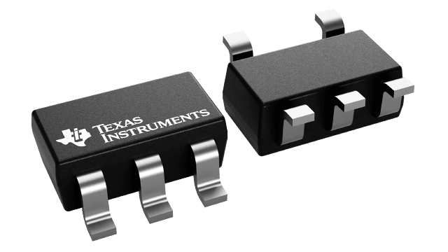
- Package: 5-pin SOT-23 (DBV) ultra-low dropout voltage
Description for the LP2985-N
The LP2985-N is a fixed-output, wide-input, low-noise, low-dropout voltage regulator supporting an input voltage range from 2.5 V to 16 V and up to 150 mA of load current. The LP2985-N supports an output range of 1.2 V to 5.0 V (new chip) and 2.5 V to 6.1 V (legacy chip).
Additionally, the LP2985-N (new chip) has a 1% output accuracy across load and temperature that can meet the needs of low-voltage microcontrollers (MCUs) and processors.
Low output noise of 30 µV RMS (with 10-nF bypass capacitors) and wide bandwidth PSRR performance of greater than 70 dB at 1 kHz and 40 dB at 1 MHz help attenuate the switching frequency of an upstream DC/DC converter and minimize post regulator filtering.
The internal soft-start time and current-limit protection reduce inrush current during start up, thus minimizing input capacitance. Standard protection features, such as overcurrent and overtemperature protection, are included.
The LP2985-N is available in a 5-pin, 2.9-mm × 1.6-mm SOT-23 (DBV) package.