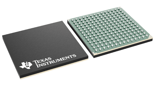
Packaging information
| Package | Pins NFBGA (NZH) | 196 |
| Operating temperature range (°C) -40 to 85 |
| Package qty | Carrier 119 | JEDEC TRAY (10+1) |
Features for the SCAN921260
- IEEE 1149.1 (JTAG) Compliant and At-Speed BIST Test Modes
- Deserializes One to Six BusLVDS Input Serial Data Streams With Embedded Clocks
- Seven Selectable Serial Inputs to Support N+1 Redundancy of Deserialized Streams
- Seventh Channel Has Single Pin Monitor Output That Reflects Input From Seventh Channel Input
- Parallel Clock Rate Up To 66 MHz
- On Chip Filtering for PLL
- High Impedance Inputs Upon Power Off (Vcc = 0V)
- Single Power Supply at +3.3V
- 196-Pin NFBGA Package (Low-Profile Ball Grid Array) Package
- Industrial Temperature Range Operation: −40 to +85
All trademarks are the property of their respective owners.
Description for the SCAN921260
The SCAN921260 integrates six deserializer devices into a single chip. The SCAN921260 can simultaneously deserialize up to six data streams that have been serialized by the Texas Instruments SCAN921023 Bus LVDS serializer. The device also includes a seventh serial input channel that serves as a redundant input.
Each deserializer block in the SCAN921260 operates independently with its own clock recovery circuitry and lock-detect signaling.
The SCAN921260 uses a single +3.3V power supply with an estimated power dissipation of 1.2W at 3.3V with a PRBS-15 pattern. Refer to the Connection Diagrams for packaging information.