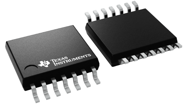
Packaging information
| Package | Pins TSSOP (PW) | 14 |
| Operating temperature range (°C) -40 to 125 |
| Package qty | Carrier 2,000 | LARGE T&R |
Features for the SN74AHC125-Q1
- Qualified for automotive applications
- EPIC™ (Enhanced-Performance Implanted CMOS) process
- Operating range 2-V to 5.5-V VCC
- Latch-up performance exceeds 250 mAper JESD 17
Description for the SN74AHC125-Q1
The SN74AHC125-Q1 is a quadruple bus buffer gate featuring independent line drivers with 3-state outputs. Each output is disabled when the associated output-enable (OE) input is high. When OE is low, the respective gate passes the data from the A input to its Y output.
To put the device in the high-impedance state during power up or power down, tie OE to VCC through a pullup resistor; the current-sinking capability of the driver determines the minimum value of the resistor.
