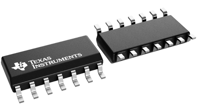
Packaging information
| Package | Pins SOIC (D) | 14 |
| Operating temperature range (°C) -40 to 125 |
| Package qty | Carrier 50 | TUBE |
Features for the SN74AHCT125
- Inputs are TTL-voltage compatible
- Latch-up performance exceeds 250mA per JESD 17
Description for the SN74AHCT125
The ’AHCT125 devices are quadruple bus buffer gates featuring independent line drivers with 3-state outputs. Each output is disabled when the associated output-enable (OE) input is high. When OE is low, the respective gate passes the data from the A input to its Y output.
For the high-impedance state during power up or power down, OE should be tied to VCC through a pullup resistor; the minimum value of the resistor is determined by the current-sinking capability of the driver.
