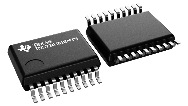
Packaging information
| Package | Pins SSOP (DB) | 20 |
| Operating temperature range (°C) -40 to 125 |
| Package qty | Carrier 2,000 | LARGE T&R |
Features for the SN74LV540A
- V CC operation of 2 V to 5.5 V
- Max t pd of 8.5 ns at 5 V
- Typical V OLP (Output Ground Bounce) < 0.8 V at V CC = 3.3 V, T A = 25°C
- Typical V OHV (Output V OH Undershoot) > 2.3 V at V CC = 3.3 V, T A = 25°C
- Supports Mixed-Mode Voltage operation on all ports
- I off supports Partial-Power-Down Mode operation
- Latch-up performance exceeds 250 mA per JESD 17
Description for the SN74LV540A
The SN74LV540A device is an octal buffer/driver designed for 2 V to 5.5 V V CC operation.
This device is ideal for driving bus lines or buffer memory address registers. It features inputs and outputs on opposite sides of the package to facilitate printed circuit board layout.
