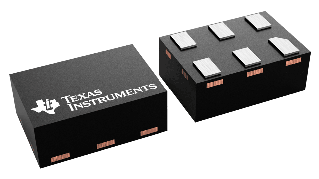
Packaging information
| Package | Pins USON (DRY) | 6 |
| Operating temperature range (°C) -40 to 125 |
| Package qty | Carrier 5,000 | LARGE T&R |
Features for the SN74LXCH1T45
- Fully configurable dual-rail design allows each port to operate from 1.1 V to 5.5 V
- Robust, glitch-free power supply sequencing
- Up to 420-Mbps support for 3.3 V to 5.0 V
- Bus hold on data inputs eliminates the need for external pull-up and pull-down resistors
- Schmitt-trigger control inputs allow for slow or noisy inputs
- Control inputs with integrated static pull-down resistors allow for floating control inputs
- High drive strength (up to 32 mA at 5 V)
- Low power consumption
- 3-µA maximum (25°C)
- 6-µA maximum (–40°C to 125°C)
- VCC isolation and VCC disconnect feature
- If either VCC supply is < 100 mV all I/O’s become high-impedance
- Ioff-float supports VCC disconnect operation
- Ioff supports partial-power-down mode operation
- Compatible with LVC family level shifters
- Control logic (DIR) are referenced to VCCA
- Operating temperature from –40°C to +125°C
- Latch-up performance exceeds 100 mA per JESD 78, class II
- ESD protection exceeds JESD 22
- 4000-V human-body model
- 1000-V charged-device model
Description for the SN74LXCH1T45
The SN74LXCH1T45 is an 1-bit, dual-supply noninverting bidirectional voltage level translation device with bus-hold circuitry. The I/O pin A and control pin (DIR) are referenced to VCCA logic levels, and the I/O pin B is referenced to VCCB logic levels. The A pin is able to accept I/O voltages ranging from 1.1 V to 5.5 V, while the B port can accept I/O voltages from 1.1 V to 5.5 V. A high on DIR allows data transmission from A to B and a low on DIR allows data transmission from B to A. See Device Functional Modes for a summary of the operation of the control logic.