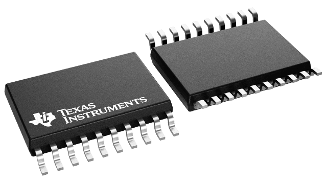
Packaging information
| Package | Pins TSSOP (PW) | 20 |
| Operating temperature range (°C) -40 to 85 |
| Package qty | Carrier 2,000 | LARGE T&R |
Features for the TLV2553
- 12-Bit-Resolution A/D Converter
- Up to 200 KSPS (150 KSPS for 3 V) Throughput
Over Operating Temperature Range With 12-Bit
Output Mode - 11 Analog Input Channels
- 3 Built-In Self-Test Modes
- Inherent Sample and Hold Function
- Linearity Error, ±1 LSB Maximum
- On-Chip Conversion Clock
- Unipolar or Bipolar Output Operation
- Programmable MSB or LSB First
- Programmable Power Down
- Programmable Output Data Length
- SPI Compatible Serial Interface With I/O Clock
Frequencies up to 15 MHz (CPOL=0, CPHA=0)
Description for the TLV2553
The TLV2553 is a 12-bit, switched-capacitor, successive-approximation, analog-to-digital converter. The ADC has three control inputs [chip select (CS), the input-output clock, and the address/control input (DATAIN)], designed for communication with the serial port of a host processor or peripheral through a serial 3-state output.
In addition to the high-speed converter and versatile control capability, the device has an on-chip 14-channel multiplexer that can select any one of 11 inputs or any one of three internal self-test voltages using configuration register 1. The sample-and-hold function is automatic. At the end of conversion, when programmed as EOC, the pin 19 output goes high to indicate that conversion is complete. The converter incorporated in the device features differential, high- impedance reference inputs that facilitate ratiometric conversion, scaling, and isolation of analog circuitry from logic and supply noise. A switched-capacitor design allows low-error conversion over the full operating temperature range.
The TLV2553I is characterized for operation from TA = –40°C to 85°C.
