Packaging information
| Package | Pins VQFN (RGB) | 20 |
| Operating temperature range (°C) -40 to 125 |
| Package qty | Carrier 250 | SMALL T&R |
Features for the TPS53317A
- TI-Proprietary Integrated MOSFET and Packaging Technology
- Supports DDR Memory Termination with up to 6-A Continuous Output Source or Sink Current
- External Tracking
- Minimum External Components Count
- to 6-V Conversion Voltage
- D-CAP+ Mode Architecture
- Supports All MLCC Output Capacitors and SP/POSCAP
- Selectable SKIP Mode or Forced CCM
- Optimized Efficiency at Light and Heavy Loads
- Selectable 600-kHz or 1-MHz Switching Frequency
- Selectable Overcurrent Limit (OCL)
- Overvoltage, Over-Temperature and Hiccup Undervoltage Protection
- Adjustable Output Voltage from to 2 V
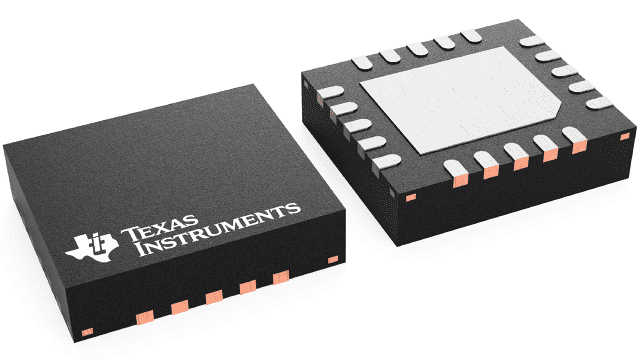
- 3.5 mm × 4 mm, 20-Pin, VQFN Package
Description for the TPS53317A
The device is a FET-integrated synchronous buck regulator designed mainly for DDR termination. It can provide a regulated output at ½ VDDQ with both sink and source capability. The device employs D-CAP+ mode operation that provides ease of use, low external component count and fast transient response. The device can also be used for other point-of-load (POL) regulation applications requiring up to 6 A. In addition, the device supports full, 6-A, output sinking current capability with tight voltage regulation.
The device features two switching frequency settings (600 kHz and 1 MHz), integrated droop support, external tracking capability, pre-bias startup, output soft discharge, integrated bootstrap switch, power good function, V5IN pin UVLO protection, and supports both ceramic and SP/POSCAP capacitors. It supports input voltages up to 6.0 V, and output voltages adjustable from to 2.0 V.
The device is available in the 3.5 mm × 4 mm, 20-pin, VQFN package (Green RoHs compliant and Pb free) with TI proprietary Integrated MOSFET and packaging technology and is specified from –40°C to 85°C.
For all available packages, see the orderable addendum at the end of the data sheet.