Packaging information
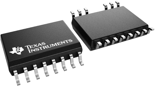
| Package | Pins SOIC (DWK) | 14 |
| Operating temperature range (°C) -40 to 125 |
| Package qty | Carrier 2,000 | LARGE T&R |
Features for the UCC21530-Q1
- AEC-Q100 qualified with:
- Device temperature grade 1
- Functional Safety Quality-Managed
- Universal: dual low-side, dual high-side or half-bridge driver
- Wide body SOIC-14 (DWK) package
- 3.3mm spacing between driver channels
- Switching parameters:
- 33ns typical propagation delay
- 20ns minimum pulse width
- 6ns maximum pulse-width distortion
- Common-mode transient immunity (CMTI) greater than 125V/ns
- 4A peak source, 6A peak sink output
- TTL and CMOS compatible inputs
- 3V to 18V input VCCI range
- Up to 25V VDD output drive supply
- 8V,12V and 17V VDD UVLO options
- Programmable overlap and dead time
- Junction temperature range –40 to +150°C
Description for the UCC21530-Q1
The UCC21530-Q1 is an isolated dual-channel gate driver with 4A source and 6A sink peak current. It is designed to drive IGBTs, Si MOSFETs, and SiC MOSFETs up to 5MHz.
The input side is isolated from the two output drivers by a 5.7kVRMS reinforced isolation barrier, with a minimum of 125V/ns common-mode transient immunity (CMTI). Internal functional isolation between the two secondary-side drivers allows a working voltage of up to 1850V.
This device can be configured as two low-side drivers, two high-side drivers, or a half-bridge driver with programmable dead time (DT). The EN pin pulled low shuts down both outputs simultaneously and allows for normal operation when left open or pulled high. As a fail-safe measure, primary-side logic failures force both outputs low.
The device accepts VDD supply voltages up to 25V. A wide input VCCI range from 3V to 18V makes the driver suitable for interfacing with both analog and digital controllers. All the supply voltage pins have under voltage lock-out (UVLO) protection.