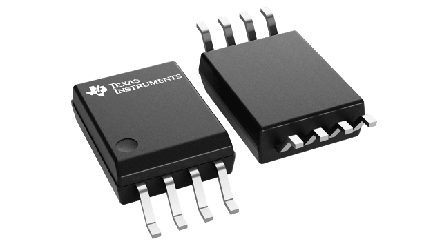
Packaging information
| Package | Pins SOIC (DWV) | 8 |
| Operating temperature range (°C) -40 to 125 |
| Package qty | Carrier 1,000 | LARGE T&R |
Features for the UCC23514
- 5.0-kVRMS single channel isolated gate driver with opto-compatible input
- Pin-to-pin, drop in upgrade for opto-isolated gate drivers
- 4.5-A source, 5.3-A sink, peak output current
- 12-V to 33-V output driver supply voltage
- Rail-to-rail output
- 105-ns (maximum) propagation delay
- 25-ns (maximum) part-to-part delay matching
- 35-ns (maximum) pulse width distortion
- 150-kV/µs (minimum) common-mode transient immunity (CMTI)
- Isolation barrier life > 50 Years
- 13-V reverse polarity voltage handling capability on input stage
- DWV package with 8.5 mm creepage
- Operating junction temperature, TJ: –40°C to +150°C
- Safety-related certifications (Planned):
- 7000-VPK reinforced isolation per DIN V VDE V0884-11: 2017-01
- 5.0-kVRMS isolation for 1 minute per UL 1577
- CQC certification per GB4943.1-2011
Description for the UCC23514
The UCC23514 is an Opto-compatible, single-channel, isolated gate driver for IGBTs, MOSFETs and SiC MOSFETs, with 4.5-A source and 5.3-A sink peak output current and 5.0-kVRMS reinforced isolation rating. The high supply voltage range of 33-V allows the use of bipolar supplies to effectively drive IGBTs and SiC power FETs. UCC23514 can drive both low side and high side power FETs. Key features and characteristics bring significant performance and reliability upgrades over standard opto-coupler based gate drivers while maintaining pin-to-pin compatibility in both schematic and layout design. Performance highlights include high common mode transient immunity (CMTI), low propagation delay, and small pulse width distortion.
Tight process control results in small part-to-part skew. The input stage is an emulated diode (e-diode) which means long term reliability and excellent aging characteristics compared to traditional LEDs. It is offered in an 8-Pin surface mount 7.5 mm x 5.85 mm (typical) SOIC package, with creepage and clearance ≥ 8.5 mm, and a mold compound from material group I which has a comparative tracking index (CTI) > 600 V. UCC23514’s high performance and reliability makes it ideal for use in all types of motor drives, solar inverters, industrial power supplies, and appliances. The higher operating temperature opens up opportunities for applications not previously able to be supported by traditional opto-couplers.
The UCC23514V option provides the gate drive output on a single terminal. For applications requiring split gate drive output, the UCC23514S version provides two separate output pins, OUTH and OUTL. The UCC23514E version suits applications requiring an UVLO referenced to a separate COM pin, which facilitates bipolar gate drive supply applications. The UCC23514M option connects the gate of the transistor to an internal clamp to prevent false turn-on caused by Miller current.
