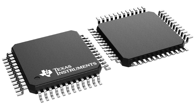
パッケージ情報
| パッケージ | ピン数 TQFP (PFB) | 48 |
| 動作温度範囲 (℃) -40 to 105 |
| パッケージ数量 | キャリア 250 | JEDEC TRAY (10+1) |
ADC08B200-Q1 の特徴
Key Specifications
|
Resolution |
8 Bits |
|
Maximum sampling frequency |
200 MSPS (min) |
|
DNL |
±0.4 LSB (typ) |
|
ENOB (fIN= 49 MHz) |
7.2 bits (typ) |
|
THD (fIN= 49 MHz) |
−53 dBc (typ) |
|
Operating, 50 MHz Input |
2 mW / Msps (typ) |
|
Power Down |
2.15 mW (typ) |
ADC08B200-Q1 に関する概要
The ADC08B200 is a high speed analog-to-digital converter (ADC) with an integrated capture buffer. The 8-bit, 200 MSPS A/D core is based upon the proven ADC08200 with integrated track-and-hold and is optimized for low power consumption. This device contains a selectable size capture buffer of up to 1,024 bytes that allows fast capture of an input signal with a slower readout rate. An on-chip clock PLL circuit provides the option of on-chip clock rate multiplication to provide the high speed sampling clock.
The ADC08B200 is resistant to latch-up and the outputs are short-circuit proof. The top and bottom of the ADC08B200's reference ladder are available for connections, enabling a wide range of input possibilities. The digital outputs are TTL/CMOS compatible with a separate output power supply pin to support interfacing with 2.7V to 3.3V logic. The digital inputs and outputs are low voltage TTL/CMOS compatible and the output data format is straight binary.
The ADC08B200Q runs on an Automotive Grade Flow and is AEC-Q100 Grade 2 Qualified.
The ADC08B200 is offered in a 48-pin plastic package (TQFP) and is specified over the extended industrial temperature range of −40°C to +105°C. An evaluation board is available to assist in the easy evaluation of the ADC08B200.