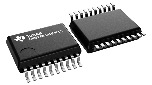
패키징 정보
| 패키지 | 핀 SSOP (DB) | 20 |
| 작동 온도 범위(°C) -40 to 85 |
| 패키지 수량 | 캐리어 2,000 | LARGE T&R |
SN74LVT240A의 주요 특징
- Supports Mixed-Mode Signal Operation (5-V Input and Output Voltages With 3.3-V VCC)
- Supports Unregulated Battery Operation Down to 2.7 V
- Typical VOLP (Output Ground Bounce)
<0.8 V at VCC = 3.3 V, TA = 25°C - Ioff and Power-Up 3-State Support Hot Insertion
- Latch-Up Performance Exceeds 100 mA Per JESD 78, Class II
- ESD Protection Exceeds JESD 22
- 2000-V Human-Body Model (A114-A)
- 200-V Machine Model (A115-A)
- 1000-V Charged-Device Model (C101)
SN74LVT240A에 대한 설명
This octal buffer and line driver is designed specifically for low-voltage (3.3-V) VCC operation, but with the capability to provide a TTL interface to a 5-V system environment.
The SN74LVT240A is organized as two 4-bit buffer/line drivers with separate output-enable (OE)\ inputs. When OE\ is low, the device passes data from the A inputs to the Y outputs. When OE\ is high, the outputs are in the high-impedance state.
When VCC is between 0 and 1.5 V, the device is in the high-impedance state during power up or power down. However, to ensure the high-impedance state above 1.5 V, OE\ should be tied to VCC through a pullup resistor; the minimum value of the resistor is determined by the current-sinking capability of the driver.
This device is fully specified for hot-insertion applications using Ioff and power-up 3-state. The Ioff circuitry disables the outputs, preventing damaging current backflow through the device when it is powered down. The power-up 3-state circuitry places the outputs in the high-impedance state during power up and power down, which prevents driver conflict.
