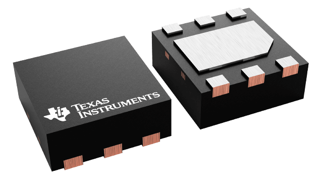
Packaging information
| Package | Pins WSON (DRV) | 6 |
| Operating temperature range (°C) -40 to 125 |
| Package qty | Carrier 3,000 | LARGE T&R |
Features for the LP5912-Q1
- Qualified for Automotive Applications
- AEC Q100-Qualified With the Following Results
- Device Temperature Grade 1: –40°C to +125°C Ambient Operating Temperature Range
- Device HBM Classification Level 2
- Device CDM Classification Level C6
- Input Voltage Range: 1.6 V to 6.5 V
- Output Voltage Range: 0.8 V to 5.5 V
- Output Current up to 500 mA
- Low Output-Voltage Noise: 12 µVRMS Typical
- PSRR at 1 kHz: 75 dB Typical
- Output Voltage Tolerance (VOUT ≥ 3.3 V): ±2%
- Low IQ (Enabled, No Load): 30 µA Typical
- Low Dropout (VOUT ≥ 3.3 V): 95 mV Typical at 500-mA Load
- Stable With 1-µF Ceramic Input and Output Capacitors
- Thermal-Overload and Short-Circuit Protection
- Reverse Current Protection
- No Noise Bypass Capacitor Required
- Output Automatic Discharge for Fast Turnoff
- Power-Good Output With 140-µs Typical Delay
- Internal Soft-Start to Limit the In-rush Current
- –40°C to +125°C Operating Junction Temperature Range
Description for the LP5912-Q1
The LP5912-Q1 is low-noise LDO that can supply up to 500 mA of output current. Designed to meet the requirements of RF and analog circuits, the LP5912-Q1 device provides low noise, high PSRR, low quiescent current, and low line and load transient response. The LP5912-Q1 offers class-leading noise performance without a noise bypass capacitor and with the ability for remote output capacitance placement.
The device is designed to work with a 1-µF input and a 1-µF output ceramic capacitor (no separate noise bypass capacitor required).
This device is available with fixed output voltages from 0.8 V to 5.5 V in 25-mV steps. Contact Texas Instruments Sales for specific voltage option needs.
For all available packages, see the Package Option Addendum (POA) at the end of this data sheet.