SBAS661C February 2015 – May 2021 ADS1262 , ADS1263
PRODUCTION DATA
- 1 Features
- 2 Applications
- 3 Description
- 4 Revision History
- 5 Device Comparison
- 6 Pin Configuration and Functions
- 7 Specifications
-
8 Parameter Measurement Information
- 8.1 Offset Temperature Drift Measurement
- 8.2 Gain Temperature Drift Measurement
- 8.3 Common-Mode Rejection Ratio Measurement
- 8.4 Power-Supply Rejection Ratio Measurement
- 8.5 Crosstalk Measurement (ADS1263)
- 8.6 Reference-Voltage Temperature-Drift Measurement
- 8.7 Reference-Voltage Thermal-Hysteresis Measurement
- 8.8 Noise Performance
-
9 Detailed Description
- 9.1 Overview
- 9.2 Functional Block Diagram
- 9.3
Feature Description
- 9.3.1 Multifunction Analog Inputs
- 9.3.2 Analog Input Description
- 9.3.3 Sensor Bias
- 9.3.4 Temperature Sensor
- 9.3.5 Power-Supply Monitor
- 9.3.6 PGA
- 9.3.7 PGA Voltage Overrange Monitors
- 9.3.8 ADC Reference Voltage
- 9.3.9 ADC1 Modulator
- 9.3.10 Digital Filter
- 9.3.11 Sensor-Excitation Current Sources (IDAC1 and IDAC2)
- 9.3.12 Level-Shift Voltage
- 9.3.13 General-Purpose Input/Output (GPIO)
- 9.3.14 Test DAC (TDAC)
- 9.3.15 ADC2 (ADS1263)
- 9.4
Device Functional Modes
- 9.4.1 Conversion Control
- 9.4.2 Conversion Latency
- 9.4.3 Programmable Time Delay
- 9.4.4 Serial Interface
- 9.4.5 Data Ready Pin (DRDY)
- 9.4.6 Conversion Data Software Polling
- 9.4.7 Read Conversion Data
- 9.4.8 ADC Clock Modes
- 9.4.9
Calibration
- 9.4.9.1 Offset and Full-Scale Calibration
- 9.4.9.2 ADC1 Offset Self-Calibration (SFOCAL1)
- 9.4.9.3 ADC1 Offset System Calibration (SYOCAL1)
- 9.4.9.4 ADC2 Offset Self-Calibration ADC2 (SFOCAL2)
- 9.4.9.5 ADC2 Offset System Calibration ADC2 (SYOCAL2)
- 9.4.9.6 ADC1 Full-Scale System Calibration (SYGCAL1)
- 9.4.9.7 ADC2 Full-Scale System Calibration ADC2 (SYGCAL2)
- 9.4.9.8 Calibration Command Procedure
- 9.4.9.9 User Calibration Procedure
- 9.4.10 Reset
- 9.4.11 Power-Down Mode
- 9.4.12 Chop Mode
- 9.5 Programming
- 9.6
Register Maps
- 9.6.1 Device Identification Register (address = 00h) [reset = x]
- 9.6.2 Power Register (address = 01h) [reset = 11h]
- 9.6.3 Interface Register (address = 02h) [reset = 05h]
- 9.6.4 Mode0 Register (address = 03h) [reset = 00h]
- 9.6.5 Mode1 Register (address = 04h) [reset = 80h]
- 9.6.6 Mode2 Register (address = 05h) [reset = 04h]
- 9.6.7 Input Multiplexer Register (address = 06h) [reset = 01h]
- 9.6.8 Offset Calibration Registers (address = 07h, 08h, 09h) [reset = 00h, 00h, 00h]
- 9.6.9 Full-Scale Calibration Registers (address = 0Ah, 0Bh, 0Ch) [reset = 40h, 00h, 00h]
- 9.6.10 IDACMUX Register (address = 0Dh) [reset = BBh]
- 9.6.11 IDACMAG Register (address = 0Eh) [reset = 00h]
- 9.6.12 REFMUX Register (address = 0Fh) [reset = 00h]
- 9.6.13 TDACP Control Register (address = 10h) [reset = 00h]
- 9.6.14 TDACN Control Register (address = 11h) [reset = 00h]
- 9.6.15 GPIO Connection Register (address = 12h) [reset = 00h]
- 9.6.16 GPIO Direction Register (address = 13h) [reset = 00h]
- 9.6.17 GPIO Data Register (address = 14h) [reset = 00h]
- 9.6.18 ADC2 Configuration Register (address = 15h) [reset = 00h]
- 9.6.19 ADC2 Input Multiplexer Register (address = 16h) [reset = 01h]
- 9.6.20 ADC2 Offset Calibration Registers (address = 17h, 18h) [reset = 00h, 00h]
- 9.6.21 ADC2 Full-Scale Calibration Registers (address = 19h, 1Ah) [reset = 00h, 40h]
- 10Application and Implementation
- 11Power Supply Recommendations
- 12Layout
- 13Device and Documentation Support
Package Options
Mechanical Data (Package|Pins)
- PW|28
Thermal pad, mechanical data (Package|Pins)
Orderable Information
9.4.2 Conversion Latency
The digital filter averages and down-samples data from the modulator to provide the final data rate (rate reduction). The order of the digital filter affects the amount of data averaging and in turn, the time delay of the conversion (or filter latency). The FIR and sinc1 filter modes are zero latency providing the conversion result in single cycle. The higher order sinc filters (sinc2, 3, 4, 5) have more than one conversion latency and therefore require more conversion cycles to provide fully settled data. Tradeoffs can be made between 50-Hz and 60-Hz line cycle rejection verses conversion latency by selection of the sinc filter order. A higher order sinc filter increases the rejection of the 50-Hz and 60-Hz line cycles, but also increases the filter latency. Filter latency is an important consideration when multiplexing (scanning) through input channels. To make sure that conversions are settled after changing channels, start a new conversion for each channel using the START pin or start command. Note if the multiplexer is changed during ongoing conversions, the conversion is stopped and restarted at the time multiplexer register is changed.
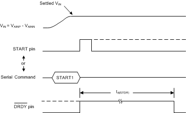
Table 9-13 lists the filter latency after starting the first conversion. Note the conversion latency depends on the filter setting. The conversion latency is illustrated in Figure 9-39. Parameter td(STDR) shows the latency from start to conversion data ready (DRDY low). Note that settled data are provided, assuming the analog input is settled before the start condition. After the first conversion is completed (in continuous conversion mode), subsequent conversions occur at the nominal data rate. The latency values are for the programmable time-delay parameter set to off (DELAY[3:0] = 000).
 Figure 9-39 Conversion Latency After
Start Condition
Figure 9-39 Conversion Latency After
Start Condition| DATA RATE (SPS) |
CONVERSION LATENCY(1) (ms) | |||||
|---|---|---|---|---|---|---|
| SINC1 | SINC2 | SINC3 | SINC4 | SINC5 | FIR | |
| 2.5 | 400.4 | 800.4 | 1,200 | 1,600 | — | 402.2 |
| 5 | 200.4 | 400.4 | 600.4 | 800.4 | — | 202.2 |
| 10 | 100.4 | 200.4 | 300.4 | 400.4 | — | 102.2 |
| 16.6 | 60.35 | 120.4 | 180.4 | 240.4 | — | — |
| 20 | 50.35 | 100.4 | 150.4 | 200.4 | — | 52.22 |
| 50 | 20.35 | 40.42 | 60.42 | 80.42 | — | — |
| 60 | 17.02 | 33.76 | 50.42 | 67.09 | — | — |
| 100 | 10.35 | 20.42 | 30.42 | 40.42 | — | — |
| 400 | 2.855 | 5.424 | 7.924 | 10.42 | — | — |
| 1200 | 1.188 | 2.091 | 2.924 | 3.758 | — | — |
| 2400 | 0.771 | 1.258 | 1.674 | 2.091 | — | — |
| 4800 | 0.563 | 0.8409 | 1.049 | 1.258 | — | — |
| 7200 | 0.494 | 0.702 | 0.841 | 0.980 | — | — |
| 14400 | — | — | — | — | 0.424 | — |
| 19200 | — | — | — | — | 0.337 | — |
| 38400 | — | — | — | — | 0.207 | — |
If using chop or IDAC rotation modes, the latency of the first conversion increases. The latency of chop and IDAC rotation modes is shown in Equation 19 and Equation 20.
In addition, chop or IDAC rotation mode can reduce the conversion data rate depending on the time-delay parameter. The 50-Hz and 60-Hz filter response nulls are not altered by chop or IDAC rotation modes. Equation 21 shows the effective data rate with the DELAY parameter.
Table 9-14 shows the first conversion latency of ADC2. The filter latency is the elapsed time after sending the START2 command before the first conversion is ready.
| DATA RATE (SPS) | CONVERSION LATENCY (ms) |
|---|---|
| 10 | 121 |
| 100 | 31.2 |
| 400 | 8.71 |
| 800 | 4.97 |
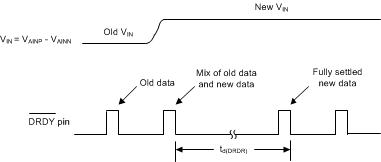
If the input signal changes while the ADC is continuously converting, the output data are a mix of old and new data, as shown in Figure 9-40. The filter latency values for settled data (td(STDR)) with an input step change while continuously converting is shown in Table 9-15. The filter latency values listed in the table (td(STDR)) assume the analog input is settled before the start of the first whole conversion period.
 Figure 9-40 ADC1 Latency Timing While
Continuously Converting
Figure 9-40 ADC1 Latency Timing While
Continuously Converting| DIGITAL FILTER | FULLY SETTLED CONVERSION td(DRDR) (1 / DR)(1) |
|---|---|
| FIR | 1 |
| Sinc1 | 1 |
| Sinc2 | 2 |
| Sinc3 | 3 |
| Sinc4 | 4 |
| Sinc5 | 5 |