SBAS661C February 2015 – May 2021 ADS1262 , ADS1263
PRODUCTION DATA
- 1 Features
- 2 Applications
- 3 Description
- 4 Revision History
- 5 Device Comparison
- 6 Pin Configuration and Functions
- 7 Specifications
-
8 Parameter Measurement Information
- 8.1 Offset Temperature Drift Measurement
- 8.2 Gain Temperature Drift Measurement
- 8.3 Common-Mode Rejection Ratio Measurement
- 8.4 Power-Supply Rejection Ratio Measurement
- 8.5 Crosstalk Measurement (ADS1263)
- 8.6 Reference-Voltage Temperature-Drift Measurement
- 8.7 Reference-Voltage Thermal-Hysteresis Measurement
- 8.8 Noise Performance
-
9 Detailed Description
- 9.1 Overview
- 9.2 Functional Block Diagram
- 9.3
Feature Description
- 9.3.1 Multifunction Analog Inputs
- 9.3.2 Analog Input Description
- 9.3.3 Sensor Bias
- 9.3.4 Temperature Sensor
- 9.3.5 Power-Supply Monitor
- 9.3.6 PGA
- 9.3.7 PGA Voltage Overrange Monitors
- 9.3.8 ADC Reference Voltage
- 9.3.9 ADC1 Modulator
- 9.3.10 Digital Filter
- 9.3.11 Sensor-Excitation Current Sources (IDAC1 and IDAC2)
- 9.3.12 Level-Shift Voltage
- 9.3.13 General-Purpose Input/Output (GPIO)
- 9.3.14 Test DAC (TDAC)
- 9.3.15 ADC2 (ADS1263)
- 9.4
Device Functional Modes
- 9.4.1 Conversion Control
- 9.4.2 Conversion Latency
- 9.4.3 Programmable Time Delay
- 9.4.4 Serial Interface
- 9.4.5 Data Ready Pin (DRDY)
- 9.4.6 Conversion Data Software Polling
- 9.4.7 Read Conversion Data
- 9.4.8 ADC Clock Modes
- 9.4.9
Calibration
- 9.4.9.1 Offset and Full-Scale Calibration
- 9.4.9.2 ADC1 Offset Self-Calibration (SFOCAL1)
- 9.4.9.3 ADC1 Offset System Calibration (SYOCAL1)
- 9.4.9.4 ADC2 Offset Self-Calibration ADC2 (SFOCAL2)
- 9.4.9.5 ADC2 Offset System Calibration ADC2 (SYOCAL2)
- 9.4.9.6 ADC1 Full-Scale System Calibration (SYGCAL1)
- 9.4.9.7 ADC2 Full-Scale System Calibration ADC2 (SYGCAL2)
- 9.4.9.8 Calibration Command Procedure
- 9.4.9.9 User Calibration Procedure
- 9.4.10 Reset
- 9.4.11 Power-Down Mode
- 9.4.12 Chop Mode
- 9.5 Programming
- 9.6
Register Maps
- 9.6.1 Device Identification Register (address = 00h) [reset = x]
- 9.6.2 Power Register (address = 01h) [reset = 11h]
- 9.6.3 Interface Register (address = 02h) [reset = 05h]
- 9.6.4 Mode0 Register (address = 03h) [reset = 00h]
- 9.6.5 Mode1 Register (address = 04h) [reset = 80h]
- 9.6.6 Mode2 Register (address = 05h) [reset = 04h]
- 9.6.7 Input Multiplexer Register (address = 06h) [reset = 01h]
- 9.6.8 Offset Calibration Registers (address = 07h, 08h, 09h) [reset = 00h, 00h, 00h]
- 9.6.9 Full-Scale Calibration Registers (address = 0Ah, 0Bh, 0Ch) [reset = 40h, 00h, 00h]
- 9.6.10 IDACMUX Register (address = 0Dh) [reset = BBh]
- 9.6.11 IDACMAG Register (address = 0Eh) [reset = 00h]
- 9.6.12 REFMUX Register (address = 0Fh) [reset = 00h]
- 9.6.13 TDACP Control Register (address = 10h) [reset = 00h]
- 9.6.14 TDACN Control Register (address = 11h) [reset = 00h]
- 9.6.15 GPIO Connection Register (address = 12h) [reset = 00h]
- 9.6.16 GPIO Direction Register (address = 13h) [reset = 00h]
- 9.6.17 GPIO Data Register (address = 14h) [reset = 00h]
- 9.6.18 ADC2 Configuration Register (address = 15h) [reset = 00h]
- 9.6.19 ADC2 Input Multiplexer Register (address = 16h) [reset = 01h]
- 9.6.20 ADC2 Offset Calibration Registers (address = 17h, 18h) [reset = 00h, 00h]
- 9.6.21 ADC2 Full-Scale Calibration Registers (address = 19h, 1Ah) [reset = 00h, 40h]
- 10Application and Implementation
- 11Power Supply Recommendations
- 12Layout
- 13Device and Documentation Support
Package Options
Mechanical Data (Package|Pins)
- PW|28
Thermal pad, mechanical data (Package|Pins)
Orderable Information
10.1.5.1 Aliasing
As with all ADCs, out-of-band input signals can fold back or alias if not band-limited. Aliasing describes the effect of input frequencies greater than ½ the sample rate folding back to the bandwidth of interest. An antialias filter placed at the ADC inputs reduces the magnitude of the aliased frequencies. The ADS1262 and ADS1263 incorporate analog and digital antialiasing filters to attenuate the aliased frequencies. There are two ranges of aliased frequencies: frequencies greater than ½ of the down-sampled output data rate (Nyquist frequency) and frequencies occurring at multiples of the modulator sample rate.
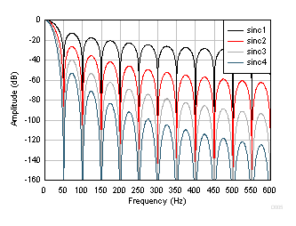
Aliasing can occur at frequencies greater than ½ the ADC output data rate. For example, at data rate of 50 SPS, aliasing occurs at frequencies greater than 25 Hz. The ADC digital filter rejects the aliased frequencies as input frequency increases. The amount of aliased frequency rejection is given by the filter type and order. Figure 10-7 illustrates the frequency response of the sinc filter. Note the sinc4 filter provides the best rejection of aliased frequencies.
 Figure 10-7 Frequency Response (50 SPS)
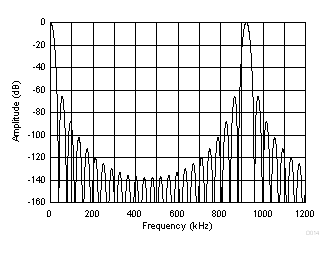
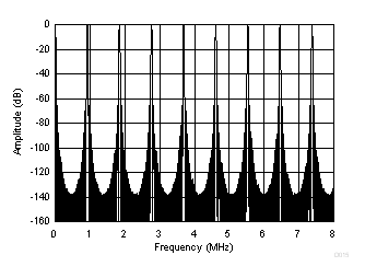
The second band of aliased frequencies occur at the ADC modulator sample rate multiples (fMOD = fCLK / 8 = 921.6 kHz, multiples = 1843.2 kHz and so on). Figure 10-8 shows the 38400 SPS frequency response plotted to 1.2 MHz. The response near dc is the signal bandwidth of interest. Observe how the digital filter response repeats on the sides of the modulator sample rate (921.6 kHz). Figure 10-9 shows the repeated response at the modulator frequency multiples = N · fMOD ± fDR, where N = multiples of fMOD starting at 1, and fDR = data rate frequency. The digital filter attenuates signal or noise up to where the response repeats. However, signal or noise occurring at the modulator sample rate is not attenuated by the digital filter and therefore, is aliased to the passband.
 Figure 10-8 Frequency Response to 1.2 MHz (38400 SPS)
 Figure 10-9 Frequency Response to 8 MHz
 (38400 SPS)
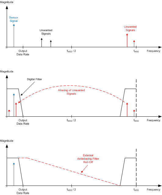
Figure 10-10 illustrates how the frequencies alias near the modulator sample rate frequency. The final figure shows the aliased frequency rejection provided by an antialias filter. The ADC incorporates an analog antialias filter with a cutoff frequency of 60 kHz that rejects the aliased frequencies.
 Figure 10-10 Alias Effect
Many sensor signals are inherently band-limited; for example, the output of a thermocouple has a limited rate of change. In this case, the sensor signal does not alias back into the pass band when using a ΔΣ ADC. However, any noise picked up along the sensor wiring or the application circuitry can potentially alias into the pass band. Power line-cycle frequency and harmonics are one common noise source. External noise is also generated from electromagnetic interference (EMI) or radio frequency interference (RFI) sources, such as nearby motors and cellular phones. Another noise source exists on the printed circuit board (PCB) in the form of clocks and other digital signals. Analog input filtering helps remove unwanted signals from affecting the measurement result. The ADC incorporates a low-pass, antialias filter with a corner frequency of 60 kHz to reduce the aliased frequencies. The filter consists of the external 4.7-nF PGA output capacitor (CAPP and CAPN pins) and internal 280-Ω resistors.
Use an input filter to provide increased rejection of aliased noise frequencies and further attenuate possible strong high-frequency interference signals. For best performance, filter strong interference frequencies at the ADC inputs. Ideally, select a low-pass corner frequency that allows frequencies within the desired bandwidth and attenuates those frequencies outside the desired bandwidth. As a result of the stable and linear dielectric characteristics, use C0G-type MLCC capacitors in analog signal filters. In applications where high energy transients can be generated, such as caused by inductive load switching, transient voltage suppressor (TVS) diodes or external ESD diodes should be used to protect the ADC inputs.