SBAS661C February 2015 – May 2021 ADS1262 , ADS1263
PRODUCTION DATA
- 1 Features
- 2 Applications
- 3 Description
- 4 Revision History
- 5 Device Comparison
- 6 Pin Configuration and Functions
- 7 Specifications
-
8 Parameter Measurement Information
- 8.1 Offset Temperature Drift Measurement
- 8.2 Gain Temperature Drift Measurement
- 8.3 Common-Mode Rejection Ratio Measurement
- 8.4 Power-Supply Rejection Ratio Measurement
- 8.5 Crosstalk Measurement (ADS1263)
- 8.6 Reference-Voltage Temperature-Drift Measurement
- 8.7 Reference-Voltage Thermal-Hysteresis Measurement
- 8.8 Noise Performance
-
9 Detailed Description
- 9.1 Overview
- 9.2 Functional Block Diagram
- 9.3
Feature Description
- 9.3.1 Multifunction Analog Inputs
- 9.3.2 Analog Input Description
- 9.3.3 Sensor Bias
- 9.3.4 Temperature Sensor
- 9.3.5 Power-Supply Monitor
- 9.3.6 PGA
- 9.3.7 PGA Voltage Overrange Monitors
- 9.3.8 ADC Reference Voltage
- 9.3.9 ADC1 Modulator
- 9.3.10 Digital Filter
- 9.3.11 Sensor-Excitation Current Sources (IDAC1 and IDAC2)
- 9.3.12 Level-Shift Voltage
- 9.3.13 General-Purpose Input/Output (GPIO)
- 9.3.14 Test DAC (TDAC)
- 9.3.15 ADC2 (ADS1263)
- 9.4
Device Functional Modes
- 9.4.1 Conversion Control
- 9.4.2 Conversion Latency
- 9.4.3 Programmable Time Delay
- 9.4.4 Serial Interface
- 9.4.5 Data Ready Pin (DRDY)
- 9.4.6 Conversion Data Software Polling
- 9.4.7 Read Conversion Data
- 9.4.8 ADC Clock Modes
- 9.4.9
Calibration
- 9.4.9.1 Offset and Full-Scale Calibration
- 9.4.9.2 ADC1 Offset Self-Calibration (SFOCAL1)
- 9.4.9.3 ADC1 Offset System Calibration (SYOCAL1)
- 9.4.9.4 ADC2 Offset Self-Calibration ADC2 (SFOCAL2)
- 9.4.9.5 ADC2 Offset System Calibration ADC2 (SYOCAL2)
- 9.4.9.6 ADC1 Full-Scale System Calibration (SYGCAL1)
- 9.4.9.7 ADC2 Full-Scale System Calibration ADC2 (SYGCAL2)
- 9.4.9.8 Calibration Command Procedure
- 9.4.9.9 User Calibration Procedure
- 9.4.10 Reset
- 9.4.11 Power-Down Mode
- 9.4.12 Chop Mode
- 9.5 Programming
- 9.6
Register Maps
- 9.6.1 Device Identification Register (address = 00h) [reset = x]
- 9.6.2 Power Register (address = 01h) [reset = 11h]
- 9.6.3 Interface Register (address = 02h) [reset = 05h]
- 9.6.4 Mode0 Register (address = 03h) [reset = 00h]
- 9.6.5 Mode1 Register (address = 04h) [reset = 80h]
- 9.6.6 Mode2 Register (address = 05h) [reset = 04h]
- 9.6.7 Input Multiplexer Register (address = 06h) [reset = 01h]
- 9.6.8 Offset Calibration Registers (address = 07h, 08h, 09h) [reset = 00h, 00h, 00h]
- 9.6.9 Full-Scale Calibration Registers (address = 0Ah, 0Bh, 0Ch) [reset = 40h, 00h, 00h]
- 9.6.10 IDACMUX Register (address = 0Dh) [reset = BBh]
- 9.6.11 IDACMAG Register (address = 0Eh) [reset = 00h]
- 9.6.12 REFMUX Register (address = 0Fh) [reset = 00h]
- 9.6.13 TDACP Control Register (address = 10h) [reset = 00h]
- 9.6.14 TDACN Control Register (address = 11h) [reset = 00h]
- 9.6.15 GPIO Connection Register (address = 12h) [reset = 00h]
- 9.6.16 GPIO Direction Register (address = 13h) [reset = 00h]
- 9.6.17 GPIO Data Register (address = 14h) [reset = 00h]
- 9.6.18 ADC2 Configuration Register (address = 15h) [reset = 00h]
- 9.6.19 ADC2 Input Multiplexer Register (address = 16h) [reset = 01h]
- 9.6.20 ADC2 Offset Calibration Registers (address = 17h, 18h) [reset = 00h, 00h]
- 9.6.21 ADC2 Full-Scale Calibration Registers (address = 19h, 1Ah) [reset = 00h, 40h]
- 10Application and Implementation
- 11Power Supply Recommendations
- 12Layout
- 13Device and Documentation Support
Package Options
Mechanical Data (Package|Pins)
- PW|28
Thermal pad, mechanical data (Package|Pins)
Orderable Information
9.3.6 PGA
The ADC1 PGA is a low-noise, programmable gain, CMOS differential-input, differential-output amplifier. The PGA extends the ADC dynamic range of sensors with low input-signal levels. The PGA provides gains of 1, 2, 4, 8 ,16, and 32. Bypass the PGA to extend the analog input range to below ground (if the AVSS pin is grounded).
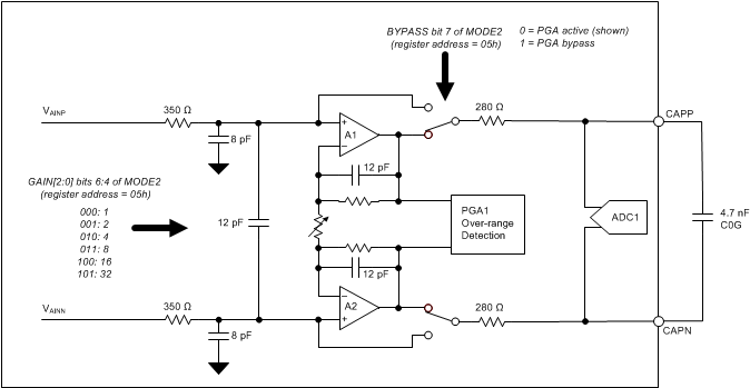
Figure 9-6 shows the PGA block diagram. The PGA consists of two chopper-stabilized amplifiers (A1 and A2), and a resistor network that is programmed to set the PGA gain. The PGA input is equipped with a high-frequency, electromagnetic-interference (EMI) input filter consisting of two 350-Ω input resistors, and several filter capacitors, as shown in the figure. Bypass the PGA to directly connect the inputs to the ADC. The PGA output is monitored by an overrange voltage monitor. The voltage monitor triggers an alarm when the absolute or differential PGA output voltage exceeds the linear range of operation. Pins CAPP and CAPN are the PGA positive and negative outputs, respectively. Connect a 4.7-nF (C0G) capacitor as shown in the figure. The capacitor provides an analog antialias filter, as well as the deglitch filter for the modulator sample pulses. Place the capacitor close to the pins using short, direct traces. Avoid running clock traces or other digital traces close to the pins.
 Figure 9-6 ADC1 PGA Block Diagram
The ADC1 full-scale voltage range is determined by the reference voltage and the PGA gain. Table 9-2 shows the full-scale voltage range verses gain for reference voltage = 2.5 V. The full-scale voltage range scales with the reference voltage and is increased or decreased by changing the reference voltage.
| GAIN[2:0] BITS OF REGISTER MODE2 | GAIN (V/V) | FULL SCALE RANGE (V)(1) |
|---|---|---|
| 000 | 1 | ±2.500 V |
| 001 | 2 | ±1.250 V |
| 010 | 4 | ±0.625 V |
| 011 | 8 | ±0.312 V |
| 100 | 16 | ±0.156 V |
| 101 | 32 | ±0.078 V |
As with many amplifiers, the PGA has an absolute input voltage range requirement that cannot be exceeded. The maximum and minimum absolute input voltages are limited by the voltage swing capability of the PGA output. The specified minimum and maximum absolute input voltages (VINP and VINN) depend on the PGA gain, the input differential voltage (VIN), and the tolerance of the analog power-supply voltages (VAVDD and VAVSS). The absolute positive and negative input voltages must be within the specified range, as shown in Equation 12:
where
- VINP, VINN = absolute input voltage
- VIN = differential input voltage = VINP - VINN
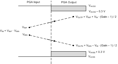
The relationship between the PGA input to the PGA output is shown graphically in Figure 9-7. The PGA output voltages (VOUTP, VOUTN) depend on the PGA gain and the input voltage magnitudes. For linear operation, the PGA output voltages must not exceed VAVDD – 0.3 or VAVSS + 0.3. Note the diagram depicts a positive differential input voltage that results in a positive differential output voltage.
 Figure 9-7 PGA
Input/Output Range
Figure 9-7 PGA
Input/Output RangeIf the PGA is bypassed, the ADC absolute input voltage range extends beyond the VAVDD and VAVSS power supplies allowing input voltages at or below ground. The absolute input voltage range when the PGA is bypassed is shown in Equation 13: