-
ADS8866 16-bit, 100-kSPS, serial interface, micropower, miniature, single-ended input, SAR analog-to-digital converter
- 1 Features
- 2 Applications
- 3 Description
- 4 Revision History
- 5 Device Comparison Table
- 6 Pin Configuration and Functions
- 7 Specifications
- 8 Parameter Measurement Information
- 9 Detailed Description
- 10Application and Implementation
- 11Power Supply Recommendations
- 12Layout
- 13Device and Documentation Support
- 14Mechanical, Packaging, and Orderable Information
- IMPORTANT NOTICE
Package Options
Mechanical Data (Package|Pins)
Thermal pad, mechanical data (Package|Pins)
- DRC|10
Orderable Information
ADS8866 16-bit, 100-kSPS, serial interface, micropower, miniature, single-ended input, SAR analog-to-digital converter
1 Features
- Sample rate: 100 kHz
- No latency output
- Unipolar, single-ended input range:
0 to +VREF - SPI™-compatible serial interface with
daisy-chain option - Excellent AC and DC performance:
- Wide operating range:
- AVDD: 2.7 V to 3.6 V
- DVDD: 1.65 V to 3.6 V
(independent of AVDD) - REF: 2.5 V to 5 V (independent of AVDD)
- Operating temperature: –40°C to +85°C
- Low-power dissipation:
- 0.7 mW at 100 kSPS
- 70 µW at 10 kSPS
- Power-down current (AVDD): 50 nA
- Full-scale step settling to 16 Bits: 1200 ns
- Packages: VSSOP-10 and VSON-10
3 Description
The ADS8866 is a 16-bit, 100-kSPS, single-ended input, analog-to-digital converter (ADC). The device operates with a 2.5-V to 5-V external reference, offering a wide selection of signal ranges without additional input signal scaling. The reference voltage setting is independent of, and can exceed, the analog supply voltage (AVDD).
The device offers an SPI-compatible serial interface that also supports daisy-chain operation for cascading multiple devices.
The device supports unipolar single-ended analog inputs in the range of –0.1 V to VREF + 0.1 V.
Device operation is optimized for very low-power operation. Power consumption directly scales with speed. This feature makes the ADS8866 excellent for lower-speed applications.
Device Information(1)
| PART NUMBER | PACKAGE | BODY SIZE (NOM) |
|---|---|---|
| ADS8866 | VSSOP (10) | 3.00 mm × 3.00 mm |
| VSON (10) | 3.00 mm × 3.00 mm |
- For all available packages, see the orderable addendum at the end of the datasheet.
Device Images
No Separate LDO Required for the ADC Supply

4 Revision History
Changes from B Revision (February 2019) to C Revision
- Added Input current row to Absolute Maximum Ratings table Go
- Changed Minimum fSCLK required to achieve rated throughputGo
- Changed Maximum tSCLK to achieve rated throughput table.Go
Changes from A Revision (December 2013) to B Revision
- Added Device Information table, ESD Ratings table, Recommended Operating Conditions table, Parametric Measurement Information section, Feature Description section, Device Functional Modes section, Application and Implementation section, Power Supply Recommendations section, Layout section, Device and Documentation Support section, and Mechanical, Packaging, and Orderable Information sectionGo
- Changed analog input from pseudo-differential to single-ended throughout documentGo
- Changed MSOP to VSSOP throughout document Go
- Changed title of Device Comparison Table from Family InformationGo
- Changed footnotes of Family Information tableGo
- Changed LSB footnote in Electrical Characteristics table to include how to convert LSB to ppm Go
- Added more information about validity of data on SCLK edges in all interface modesGo
- Changed diagrams and text for better explanation of the daisy-chain feature in the Daisy-Chain Mode sectionGo
- Changed Equation 1 and Equation 2Go
- Changed Charge-Kickback Filter section title and functionality description Go
Changes from * Revision (May 2013) to A Revision
- Changed sub-bullets of AC and DC performance Features bulletGo
- Changed Full-scale step settling Features bulletGo
- Deleted last two Applications bulletsGo
- Changed Description sectionGo
- Changed front page graphicGo
- Added Family Information, Absolute Maximum Ratings, and Thermal Information tablesGo
- Added Pin Configurations sectionGo
- Added Electrical Characteristics tableGo
- Added Timing Characteristics sectionGo
- Added Typical Characteristics sectionGo
5 Device Comparison Table
| THROUGHPUT | 18-BIT, TRUE-DIFFERENTIAL | 16-BIT, SINGLE-ENDED | 16-BIT, TRUE-DIFFERENTIAL |
|---|---|---|---|
| 100 kSPS | ADS8887 | ADS8866 | ADS8867 |
| 250 kSPS | — | ADS8339(1) | — |
| 400 kSPS | ADS8885 | ADS8864 | ADS8865 |
| 500 kSPS | — | ADS8319(1) | ADS8318(1)(2) |
| 680 kSPS | ADS8883 | ADS8862 | ADS8863 |
| 1 MSPS | ADS8881 | ADS8860 | ADS8861 |
6 Pin Configuration and Functions
Pin Functions
| PIN | TYPE | DESCRIPTION | |
|---|---|---|---|
| NAME | NO. | ||
| AINN | 4 | Analog input | Inverting analog signal input |
| AINP | 3 | Analog input | Noninverting analog signal input |
| AVDD | 2 | Analog | Analog power supply. This pin must be decoupled to GND with a 1-µF capacitor. |
| CONVST | 6 | Digital input | Convert input. This pin also functions as the CS input in 3-wire interface mode; see the Description and Timing Requirements sections for more details. |
| DIN | 9 | Digital input | Serial data input. The DIN level at the start of a conversion selects the mode of operation (such as CS or daisy-chain mode). This pin also serves as the CS input in 4-wire interface mode; see the Description and Timing Requirements sections for more details. |
| DOUT | 7 | Digital output | Serial data output |
| DVDD | 10 | Power supply | Digital interface power supply. This pin must be decoupled to GND with a 1-µF capacitor. |
| GND | 5 | Analog, digital | Device ground. Note that this pin is a common ground pin for both the analog power supply (AVDD) and digital I/O supply (DVDD). The reference return line is also internally connected to this pin. |
| REF | 1 | Analog | Positive reference input. This pin must be decoupled with a 10-µF or larger capacitor. |
| SCLK | 8 | Digital input | Clock input for serial interface. Data output (on DOUT) are synchronized with this clock. |
| Thermal pad | — | Exposed thermal pad (only for the DRC package option). Texas Instruments recommends connecting the thermal pad to the printed circuit board (PCB) ground. | |
7 Specifications
7.1 Absolute Maximum Ratings
over operating free-air temperature range (unless otherwise noted)(1)7.2 ESD Ratings
| VALUE | UNIT | |||
|---|---|---|---|---|
| V(ESD) | Electrostatic discharge | Human-body model (HBM), per ANSI/ESDA/JEDEC JS-001(1) | ±2000 | V |
| Charged-device model (CDM), per JEDEC specification JESD22-C101(2) | ±500 | |||
7.3 Recommended Operating Conditions
over operating free-air temperature range (unless otherwise noted)| MIN | NOM | MAX | UNIT | ||
|---|---|---|---|---|---|
| AVDD | Analog power supply | 3 | V | ||
| DVDD | Digital power supply | 3 | V | ||
| VREF | Reference voltage | 5 | V | ||
7.4 Thermal Information
| THERMAL METRIC(1) | ADS8866 | UNIT | ||
|---|---|---|---|---|
| DGS (VSSOP) | DRC (VSON) | |||
| 10 PINS | 10 PINS | |||
| RθJA | Junction-to-ambient thermal resistance | 151.9 | 111.1 | °C/W |
| RθJC(top) | Junction-to-case (top) thermal resistance | 45.4 | 46.4 | °C/W |
| RθJB | Junction-to-board thermal resistance | 72.2 | 45.9 | °C/W |
| ψJT | Junction-to-top characterization parameter | 3.3 | 3.5 | °C/W |
| ψJB | Junction-to-board characterization parameter | 70.9 | 45.5 | °C/W |
| RθJC(bot) | Junction-to-case (bottom) thermal resistance | N/A | N/A | °C/W |
7.5 Electrical Characteristics
all minimum and maximum specifications are at AVDD = 3 V, DVDD = 3 V, VREF = 5 V, and fSAMPLE = 100 kSPS over the operating free-air temperature range (unless otherwise noted); typical specifications are at TA = 25°C, AVDD = 3 V, and DVDD = 3 V| PARAMETER | TEST CONDITIONS | MIN | TYP | MAX | UNIT | |||
|---|---|---|---|---|---|---|---|---|
| ANALOG INPUT | ||||||||
| Full-scale input span(1) | AINP – AINN | 0 | VREF | V | ||||
| Operating input range(1) | AINP | –0.1 | VREF + 0.1 | V | ||||
| AINN | –0.1 | + 0.1 | ||||||
| CI | Input capacitance | AINP and AINN terminal to GND | 59 | pF | ||||
| Input leakage current | During acquisition for dc input | 5 | nA | |||||
| EXTERNAL REFERENCE INPUT | ||||||||
| VREF | Input range | 2.5 | 5 | V | ||||
| Reference input current | During conversion, 100-kHz sample rate, mid-code | 35 | μA | |||||
| Reference leakage current | 250 | nA | ||||||
| CREF | Decoupling capacitor at the REF input | 10 | 22 | µF | ||||
| SYSTEM PERFORMANCE | ||||||||
| Resolution | 16 | Bits | ||||||
| NMC | No missing codes | 16 | Bits | |||||
| DNL | Differential linearity | –0.99 | ±0.6 | 1 | LSB(2) | |||
| INL | Integral linearity(5) | –2 | ±0.8 | 2 | LSB(2) | |||
| EO | Offset error(3) | –4 | ±1 | 4 | mV | |||
| Offset error drift with temperature | ±1.5 | µV/°C | ||||||
| EG | Gain error | –0.01 | ±0.005 | 0.01 | %FSR | |||
| Gain error drift with temperature | ±0.15 | ppm/°C | ||||||
| CMRR | Common-mode rejection ratio | With common-mode input signal = 5 VPP at dc | 90 | 100 | dB | |||
| PSRR | Power-supply rejection ratio | At mid-code | 80 | dB | ||||
| Transition noise | 0.5 | LSB | ||||||
| SAMPLING DYNAMICS | ||||||||
| tconv | Conversion time | 500 | 8800 | ns | ||||
| tACQ | Acquisition time | 1200 | ns | |||||
| Maximum throughput rate
with or without latency |
100 | kHz | ||||||
| Aperture delay | 4 | ns | ||||||
| Aperture jitter, RMS | 5 | ps | ||||||
| Step response | Settling to 16-bit accuracy | 1200 | ns | |||||
| Overvoltage recovery | Settling to 16-bit accuracy | 1200 | ns | |||||
| DYNAMIC CHARACTERISTICS | ||||||||
| SINAD | Signal-to-noise + distortion(7) | At 1 kHz, VREF = 5 V | 90.5 | 92.9 | dB | |||
| At 10 kHz, VREF = 5 V | 92.9 | |||||||
| At 49 kHz, VREF = 5 V | 88.2 | |||||||
| SNR | Signal-to-noise ratio(7) | At 1 kHz, VREF = 5 V | 92 | 93 | dB | |||
| At 10 kHz, VREF = 5 V | 93 | |||||||
| At 49 kHz, VREF = 5 V | 88.5 | |||||||
| THD | Total harmonic distortion(7)(4) | At 1 kHz, VREF = 5 V | –108 | dB | ||||
| At 10 kHz, VREF = 5 V | –108 | |||||||
| At 49 kHz, VREF = 5 V | –101 | |||||||
| SFDR | Spurious-free dynamic range(7) | At 1 kHz, VREF = 5 V | 108 | dB | ||||
| At 10 kHz, VREF = 5 V | 108 | |||||||
| At 49 kHz, VREF = 5 V | 101 | |||||||
| BW–3dB | –3-dB small-signal bandwidth | 30 | MHz | |||||
| POWER-SUPPLY REQUIREMENTS | ||||||||
| Power-supply voltage | AVDD | Analog supply | 2.7 | 3 | 3.6 | V | ||
| DVDD | Digital supply range | 1.65 | 1.8 | 3.6 | ||||
| Supply current | AVDD | 100-kHz sample rate, AVDD = 3 V | 0.23 | 0.4 | mA | |||
| PVA | Power dissipation | 100-kHz sample rate, AVDD = 3 V | 0.7 | 1.2 | mW | |||
| 10-kHz sample rate, AVDD = 3 V | 70 | μW | ||||||
| IAPD | Device power-down current(6) | 50 | nA | |||||
| DIGITAL INPUTS: LOGIC FAMILY (CMOS) | ||||||||
| VIH | High-level input voltage | 1.65 V < DVDD < 2.3 V | 0.8 × DVDD | DVDD + 0.3 | V | |||
| 2.3 V < DVDD < 3.6 V | 0.7 × DVDD | DVDD + 0.3 | ||||||
| VIL | Low-level input voltage | 1.65 V < DVDD < 2.3 V | –0.3 | 0.2 × DVDD | V | |||
| 2.3 V < DVDD < 3.6 V | –0.3 | 0.3 × DVDD | ||||||
| ILK | Digital input leakage current | ±10 | ±100 | nA | ||||
| DIGITAL OUTPUTS: LOGIC FAMILY (CMOS) | ||||||||
| VOH | High-level output voltage | IO = 500-μA source, CLOAD = 20 pF | 0.8 × DVDD | DVDD | V | |||
| VOL | Low-level output voltage | IO = 500-μA sink, CLOAD = 20 pF | 0 | 0.2 × DVDD | V | |||
| TEMPERATURE RANGE | ||||||||
| TA | Operating free-air temperature | –40 | 85 | °C | ||||
7.6 Timing Requirements: 3-Wire Operation
all specifications are at AVDD = 3 V, DVDD = 3 V, and over the operating free-air temperature range (unless otherwise noted)7.7 Timing Requirements: 4-Wire Operation
all specifications are at AVDD = 3 V, DVDD = 3 V, and over the operating free-air temperature range (unless otherwise noted)| MIN | TYP | MAX | UNIT | |||
|---|---|---|---|---|---|---|
| tACQ | Acquisition time | 1200 | ns | |||
| tconv | Conversion time | 500 | 8800 | ns | ||
| 1/fsample | Time between conversions | 10000 | ns | |||
| twh-DI | Pulse duration: DIN high | 10 | ns | |||
| twl-CNV | Pulse width: CONVST low | 20 | ns | |||
| td-DI-DO | Delay time: DIN low to MSB valid | 12.3 | ns | |||
| td-DI-DOhz | Delay time: DIN high or last SCLK falling edge to DOUT 3-state | 13.2 | ns | |||
| tsu-DI-CNV | Setup time: DIN high to CONVST rising edge | 7.5 | ns | |||
| th-DI-CNV | Hold time: DIN high from CONVST rising edge | 0 | ns | |||
7.8 Timing Requirements: Daisy-Chain
all specifications are at AVDD = 3 V, DVDD = 3 V, and over the operating free-air temperature range (unless otherwise noted)| MIN | TYP | MAX | UNIT | |||
|---|---|---|---|---|---|---|
| tACQ | Acquisition time | 1200 | ns | |||
| tconv | Conversion time | 500 | 8800 | ns | ||
| 1/fsample | Time between conversions | 10000 | ns | |||
| tsu-CK-CNV | Setup time: SCLK valid to CONVST rising edge | 5 | ns | |||
| th-CK-CNV | Hold time: SCLK valid from CONVST rising edge | 5 | ns | |||
| tsu-DI-CNV | Setup time: DIN low to CONVST rising edge (see Figure 2) | 7.5 | ns | |||
| th-DI-CNV | Hold time: DIN low from CONVST rising edge | 0 | ns | |||
| tsu-DI-CK | Setup time: DIN valid to SCLK falling edge | 1.5 | ns | |||
 Figure 1. 3-Wire Operation: CONVST Functions as Chip Select
  Figure 2. 4-Wire Operation: DIN Functions as Chip Select
  Figure 3. Daisy-Chain Operation: Two Devices
 7.9 Typical Characteristics
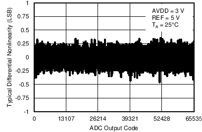
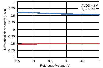
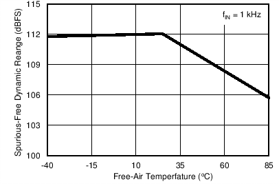
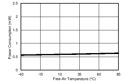
at TA = 25°C, AVDD = 3 V, DVDD = 3 V, VREF = 5 V, and fSAMPLE = 100 kSPS (unless otherwise noted)


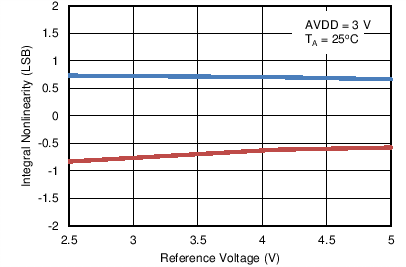


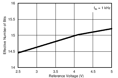


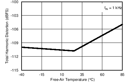


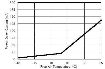


Nonlinearity (Minimum and Maximum)






8 Parameter Measurement Information
8.1 Equivalent Circuits
 Figure 37. Load Circuit for Digital Interface Timing
  Figure 38. Voltage Levels for Timing
 9 Detailed Description
9.1 Overview
The ADS8866 is a high-speed, successive approximation register (SAR), analog-to-digital converter (ADC) from a 16- and 18-bit device family. This compact device features high performance. Power consumption is inherently low and scales linearly with sampling speed. The architecture is based on charge redistribution that inherently includes a sample-and-hold (S/H) function.
The ADS8866 supports a single-ended analog input across two pins (INP and INN). When a conversion is initiated, the differential input on these pins is sampled on the internal capacitor array. While a conversion is in progress, both the INP and INN inputs are disconnected from the internal circuit.
The ADS8866 uses an internal clock to perform conversions. The device reconnects the sampling capacitors to the INP and INN pins after conversion and then enters an acquisition phase. During the acquisition phase, the device is powered down and the conversion result can be read.
The device digital output is available in SPI-compatible format, thus making interfacing with microprocessors, digital signal processors (DSPs), or field-programmable gate arrays (FPGAs) easy.
9.2 Functional Block Diagram
Figure 39 shows the detailed functional block diagram for the device.
 Figure 39. Detailed Block Diagram
 9.3 Feature Description
9.3.1 Analog Input
As shown in Figure 39, the device features a single-ended analog input. AINP can swing from GND – 0.1 V to VREF + 0.1 V and AINN can swing from GND – 0.1 V to GND + 0.1 V. Both positive and negative inputs are individually sampled on 55-pF sampling capacitors and the device converts for the voltage difference between the two sampled values: VINP – VINN. The single-ended signal range is 0 V to VREF.
Figure 40 shows an equivalent circuit of the input sampling stage. The sampling switch is represented by a 96-Ω resistance in series with the ideal switch; see the ADC Input Driver section for more details on the recommended driving circuits.
 Figure 40. Input Sampling Stage Equivalent Circuit
 Figure 39 and Figure 40 illustrate electrostatic discharge (ESD) protection diodes to REF and GND from both analog inputs. Make sure that these diodes do not turn on by keeping the analog inputs within the specified range.
9.3.2 Reference
The device operates with an external reference voltage and switches binary-weighted capacitors onto the reference terminal (REF pin) during the conversion process. The switching frequency is proportional to the internal conversion clock frequency but the dynamic charge requirements are a function of the absolute value of the input voltage and reference voltage. This dynamic load must be supported by a reference driver circuit without degrading the noise and linearity performance of the device. During the acquisition process, the device automatically powers down and does not take any dynamic current from the external reference source. The basic circuit diagram for such a reference driver circuit for precision ADCs is shown in Figure 41; see the ADC Reference Driver section for more details on the application circuits.
 Figure 41. Reference Driver Schematic
 9.3.3 Clock
The device uses an internal clock for conversion. Conversion duration may vary but is bounded by the minimum and maximum value of tconv, as specified in the Timing Requirements section. An external SCLK is only used for a serial data read operation. Data are read after a conversion completes and when the device is in acquisition phase for the next sample.
9.3.4 ADC Transfer Function
The ADS8866 is a unipolar, single-ended input device. The device output is in straight binary format.
Figure 42 shows ideal characteristics for the device. The full-scale range for the ADC input (AINP – AINN) is equal to the reference input voltage to the ADC (VREF). One LSB is equal to [(VREF / 216)].
 Figure 42. Single-Ended Transfer Characteristics
 9.4 Device Functional Modes
The ADS8866 is a low pin-count device. However, the device offers three different options for interfacing with the digital host.
These options can be broadly classified as being either CS mode (in either a 3- or 4-wire interface) or daisy-chain mode. The device operates in CS mode if DIN is high at the CONVST rising edge. If DIN is low at the CONVST rising edge, or if DIN and CONVST are connected together, the device operates in daisy-chain mode.
The 3-wire interface in CS mode is useful for applications that need galvanic isolation on-board. The 4-wire interface in CS mode allows the user to sample the analog input independent of the serial interface timing and, therefore, allows easier control of an individual device while having multiple, similar devices on-board. The daisy-chain mode is provided to hook multiple devices in a chain similar to a shift register and is useful in reducing component count and the number of signal traces on the board.
9.4.1 CS Mode
CS mode is selected if DIN is high at the CONVST rising edge. There are three different interface options available in this mode: 3-wire CS mode, and 4-wire CS mode. The following sections discuss these interface options in detail.
9.4.1.1 3-Wire CS Mode
This interface option is most useful when a single ADC is connected to an SPI-compatible digital host. In this interface option, DIN can be connected to DVDD and CONVST functions as CS (as shown in Figure 43). As shown in Figure 44, a CONVST rising edge forces DOUT to 3-state, samples the input signal, and causes the device to enter a conversion phase. Conversion is done with the internal clock and continues regardless of the state of CONVST. As a result, CONVST (functioning as CS) can be pulled low after the start of the conversion to select other devices on the board. However, CONVST must return high before the minimum conversion time (tconv-min) elapses and is held high until the maximum possible conversion time (tconv-max) elapses.
 Figure 43. Connection Diagram: 3-Wire CS Mode (DIN = 1)
  Figure 44. Interface Timing Diagram: 3-Wire CS Mode (DIN = 1)
 When conversion is complete, the device enters an acquisition phase and powers down. CONVST (functioning as CS) can be brought low after the maximum conversion time (tconv-max) elapses. On the CONVST falling edge, DOUT comes out of 3-state and the device outputs the MSB of the data. The lower data bits are output on subsequent SCLK falling edges. Data can be read at either SCLK falling or rising edges. Note that with any SCLK frequency, reading data at SCLK falling edge requires the digital host to clock in the data during the th_CK_DO-min time frame. DOUT goes to 3-state after the 16th SCLK falling edge or when CONVST goes high, whichever occurs first.
9.4.1.2 4-Wire CS Mode
This interface option is useful when one or more ADCs are connected to an SPI-compatible digital host. Figure 45 shows the connection diagram for single ADC; see Figure 47 for the connection diagram for two ADCs.
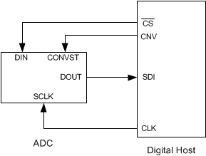 Figure 45. Connection Diagram: Single ADC With 4-Wire CS Mode
 In this interface option, DIN is controlled by the digital host and functions as CS. As shown in Figure 46, with DIN high, a CONVST rising edge selects CS mode, forces DOUT to 3-state, samples the input signal, and causes the device to enter a conversion phase. In this interface option, CONVST must be held at a high level from the start of the conversion until all data bits are read. Conversion is done with the internal clock and continues regardless of the state of DIN. As a result, DIN (functioning as CS) can be pulled low to select other devices on the board. However, DIN must be pulled high before the minimum conversion time (tconv-min) elapses and remains high until the maximum possible conversion time (tconv-max) elapses.
 Figure 46. Interface Timing Diagram: Single ADC With 4-Wire CS Mode
 When conversion is complete, the device enters acquisition phase and powers down. DIN (functioning as CS) can be brought low after the maximum conversion time (tconv-max) elapses. On the DIN falling edge, DOUT comes out of 3-state and the device outputs the MSB of the data. The lower data bits are output on subsequent SCLK falling edges. Data can be read at either SCLK falling or rising edges. Note that with any SCLK frequency, reading data at SCLK falling edge requires the digital host to clock in the data during the th_CK_DO-min time frame. DOUT goes to 3-state after the 16th SCLK falling edge or when DIN goes high, whichever occurs first.
As shown in Figure 47, multiple devices can be hooked together on the same data bus. In this case, as shown in Figure 48, the DIN of the second device (functioning as CS for the second device) can go low after the first device data are read and the DOUT of the first device is in 3-state.
Care must be taken so that CONVST and DIN are not both low together at any time during the cycle.
 Figure 47. Connection Diagram: Two ADCs With 4-Wire CS Mode
 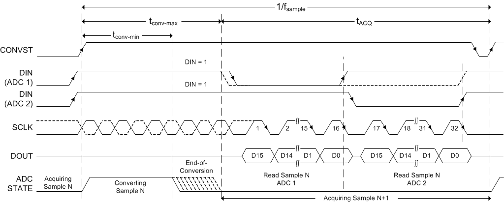 Figure 48. Interface Timing Diagram: Two ADCs With 4-Wire CS Mode
 9.4.2.1 Daisy-Chain Mode
This interface option is most useful in applications where multiple ADC devices are used but the digital host has limited interfacing capability. Figure 49 shows a connection diagram with N ADCs connected in the daisy-chain. The CONVST pins of all ADCs in the chain are connected together and are controlled by a single pin of the digital host. Similarly, the SCLK pins of all ADCs in the chain are connected together and are controlled by a single pin of the digital host. The DIN pin for ADC 1 (DIN-1) is connected to GND. The DOUT pin of ADC 1 (DOUT-1) is connected to the DIN pin of ADC 2 (DIN-2), and so on. The DOUT pin of the last ADC in the chain (DOUT-N) is connected to the SDI pin of the digital host.
 Figure 49. Connection Diagram: Daisy-Chain Mode (DIN = 0)
 As shown in Figure 50, the device DOUT pin is driven low when DIN and CONVST are low together. With DIN low, a CONVST rising edge selects daisy-chain mode, samples the analog input, and causes the device to enter a conversion phase. In this interface option, CONVST must remain high from the start of the conversion until all data bits are read. When started, the conversion continues regardless of the state of SCLK, however SCLK must be low at the CONVST rising edge.
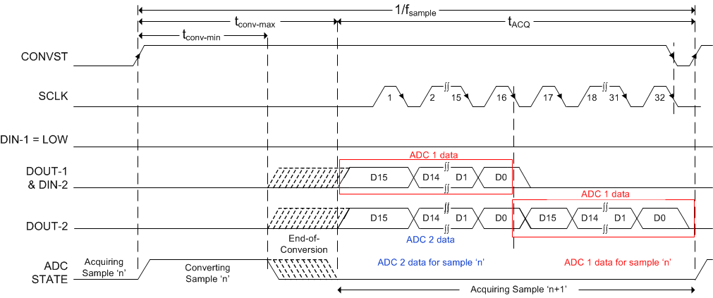 Figure 50. Interface Timing Diagram: For Two Devices in Daisy-Chain Mode
 At the end of conversion, every ADC in the chain loads its own conversion result into the internal, 16-bit, shift register and also outputs the MSB bit of this conversion result on its own DOUT pin. All ADCs enter an acquisition phase and power-down. On every subsequent SCLK falling edge, the internal shift register of each ADC latches the data available on its DIN pin and shifts out the next bit of data on its DOUT pin. Therefore, the digital host receives the data of ADC N, followed by the data of ADC N–1, and so on (in MSB-first fashion). A total of 16 x N SCLK falling edges are required to capture the outputs of all N devices in the chain. Data can be read at either SCLK falling or rising edges. Note that with any SCLK frequency, reading data at SCLK falling edge requires the digital host to clock in the data during the th_CK_DO-min time frame.
10 Application and Implementation
NOTE
Information in the following applications sections is not part of the TI component specification, and TI does not warrant its accuracy or completeness. TI’s customers are responsible for determining suitability of components for their purposes. Customers should validate and test their design implementation to confirm system functionality.
10.1 Application Information
The two primary circuits required to maximize the performance of a high-precision, successive approximation register (SAR), analog-to-digital converter (ADC) are the input driver and the reference driver circuits. This section details some general principles for designing these circuits, followed by some application circuits designed using the ADS8866.
10.1.1 ADC Reference Driver
The external reference source to the ADS8866 must provide low-drift and very accurate voltage for the ADC reference input and support the dynamic charge requirements without affecting the noise and linearity performance of the device. The output broadband noise of most references can be in the order of a few hundred μVRMS. Therefore, to prevent any degradation in the noise performance of the ADC, the output of the voltage reference must be appropriately filtered by using a low-pass filter with a cutoff frequency of a few hundred hertz.
After band-limiting the noise of the reference circuit, the next important step is to design a reference buffer that can drive the dynamic load posed by the reference input of the ADC. The reference buffer must regulate the voltage at the reference pin such that the value of VREF stays within the 1-LSB error at the start of each conversion. This condition necessitates the use of a large capacitor, CBUF_FLT (see Figure 41) for regulating the voltage at the reference input of the ADC. The amplifier selected to drive the reference pin must have an extremely low offset and temperature drift with a low output impedance to drive the capacitor at the ADC reference pin without any stability issues.
10.1.2 ADC Input Driver
The input driver circuit for a high-precision ADC mainly consists of two parts: a driving amplifier and a fly-wheel RC filter. The amplifier is used for signal conditioning of the input voltage and its low output impedance provides a buffer between the signal source and the switched capacitor inputs of the ADC. The RC filter helps attenuate the sampling charge injection from the switched-capacitor input stage of the ADC and functions as an antialiasing filter to band-limit the wideband noise contributed by the front-end circuit. Careful design of the front-end circuit is critical to meet the linearity and noise performance of a high-precision, 16-bit ADC such as the ADS8866.
10.1.2.1 Input Amplifier Selection
Selection criteria for the input amplifiers is highly dependent on the input signal type as well as the performance goals of the data acquisition system. Some key amplifier specifications to consider while selecting an appropriate amplifier to drive the inputs of the ADC are:
- Small-signal bandwidth. Select the small-signal bandwidth of the input amplifiers to be as high as possible after meeting the power budget of the system. Higher bandwidth reduces the closed-loop output impedance of the amplifier, thus allowing the amplifier to more easily drive the low cutoff frequency RC filter (see the Antialiasing Filter section) at the inputs of the ADC. Higher bandwidth also minimizes the harmonic distortion at higher input frequencies. In order to maintain the overall stability of the input driver circuit, select the amplifier bandwidth as described in Equation 1:
- Noise. Noise contribution of the front-end amplifiers must be as low as possible to prevent any degradation in SNR performance of the system. As a rule of thumb, to ensure that the noise performance of the data acquisition system is not limited by the front-end circuit, the total noise contribution from the front-end circuit must be kept below 20% of the input-referred noise of the ADC. Noise from the input driver circuit is band-limited by designing a low cutoff frequency RC filter, as explained in Equation 2.
- V1 / f_AMP_PP is the peak-to-peak flicker noise in µV,
- en_RMS is the amplifier broadband noise density in nV/√Hz,
- f–3dB is the 3-dB bandwidth of the RC filter, and
- NG is the noise gain of the front-end circuit, which is equal to 1 in a buffer configuration.
- Distortion. Both the ADC and the input driver introduce nonlinearity in a data acquisition block. As a rule of thumb, to ensure that the distortion performance of the data acquisition system is not limited by the front-end circuit, the distortion of the input driver must be at least 10 dB lower than the distortion of the ADC, as shown in Equation 3.
- Settling Time. For dc signals with fast transients that are common in a multiplexed application, the input signal must settle within an 16-bit accuracy at the device inputs during the acquisition time window. This condition is critical to maintain the overall linearity performance of the ADC. Typically, the amplifier data sheets specify the output settling performance only up to 0.1% to 0.001%, which may not be sufficient for the desired 16-bit accuracy. Therefore, always verify the settling behavior of the input driver by TINA™-SPICE simulations before selecting the amplifier.


where

10.1.2.2 Charge-Kickback Filter
The charge-kickback filter is an RC filter at the input pins of the ADC that filters the broadband noise from the front-end drive circuitry and attenuates the sampling charge injection from the switched-capacitor input stage of the ADC. As shown in Figure 51, a filter capacitor (CFLT) is connected from each input pin of the ADC to ground. This capacitor helps reduce the sampling charge injection and provides a charge bucket to quickly charge the internal sample-and-hold capacitors during the acquisition process. Generally, the value of this capacitor must be at least 20 times the specified value of the ADC sampling capacitance. For the ADS8866, the input sampling capacitance is equal to 59 pF; therefore, for optimal performance, keep CFLT greater than 590 pF. This capacitor must be a COG- or NPO-type. The type of dielectric used in COG or NPO ceramic capacitors provides the most stable electrical properties over voltage, frequency, and temperature changes.
Driving capacitive loads can degrade the phase margin of the input amplifier, thus making the amplifier marginally unstable. To avoid amplifier stability issues, series isolation resistors (RFLT) are used at the output of the amplifiers. A higher value of RFLT helps with amplifier stability, but adds distortion as a result of interactions with the nonlinear input impedance of the ADC. Distortion increases with source impedance, input signal frequency, and input signal amplitude. Therefore, the selection of RFLT requires balancing the stability of the driver amplifier and distortion performance of the design. Always verify the stability and settling behavior of the driving amplifier and charge-kickback filter by a TINA-TI™ SPICE simulation. Keep the tolerance of the selected resistors less than 1% to keep the inputs balanced.
 Figure 51. Charge-Kickback Filter
 This section describes some common application circuits using the ADS8866. These data acquisition (DAQ) blocks are optimized for specific input types and performance requirements of the system. For simplicity, power-supply decoupling capacitors are not shown in these circuit diagrams; see the Power-Supply Decoupling section for suggested guidelines.
10.2 Typical Applications
10.2.1 DAQ Circuit for a 10-µs, Full-Scale Step Response
 Figure 52. DAQ Circuit for a 10-µs, Full-Scale Step Response
 10.2.1.1 Design Requirements
Step input signals are common in multiplexed applications when switching between different channels. In the worst-case scenario, one channel is at the negative full-scale (NFS) and the other channel is at the positive full-scale (PFS) voltage, in which case the step size is the full-scale range (FSR) of the ADC when the MUX channel is switched.
Design an application circuit optimized for using the ADS8866 to achieve
- Full-scale step input settling to 16-bit accuracy and
- INL of < ±2 LSB and
- Maximum specified throughput of 100 kSPS
10.2.1.2 Detailed Design Procedure
The application circuit is shown in Figure 52.
In such applications, the primary design requirement is to ensure that the full-scale step input signal settles to 16-bit accuracy at the ADC inputs. This condition is critical to achieve the excellent linearity specifications of the ADC. Therefore, the bandwidth of the charge-kickback RC filter must be large enough to allow optimal settling of the input signal during the ADC acquisition time. The filter capacitor helps reduce the sampling charge injection at the ADC inputs, but degrades the phase margin of the driving amplifier, thereby leading to stability issues. Amplifier stability is maintained by the series isolation resistor.
During the conversion process, binary-weighted capacitors are switched onto the REF pin. In order to support this dynamic load the output of the voltage reference must be buffered with a low-output impedance (high-bandwidth) buffer.
The REF60xx family of voltage references are able to maintain an output voltage within 1 LSB (16-bit) with minimal droop, even during the first conversion while driving the REF pin of the ADS8866. This feature is useful in burst-mode, event-triggered, equivalent-time sampling, and variable-sampling-rate data-acquisition systems.
For the input driving amplifiers, key specifications include rail-to-rail input and output swing, high bandwidth, high slew rate, and fast settling time. The CMOS amplifier meets all these specification requirements for this circuit with a single-supply and low quiescent current. The component values of the antialiasing filter are selected to meet the settling requirements of the system as well as to maintain the stability of the input driving amplifiers.
10.2.2 DAQ Circuit for Lowest Distortion and Noise Performance at 100 kSPS
 Figure 53. DAQ Circuit for Lowest Distortion and Noise at 100 kSPS